
onsemi (Ansemi)
画像はイメージの場合もございます。
商品詳細は仕様をご覧ください。
商品詳細は仕様をご覧ください。

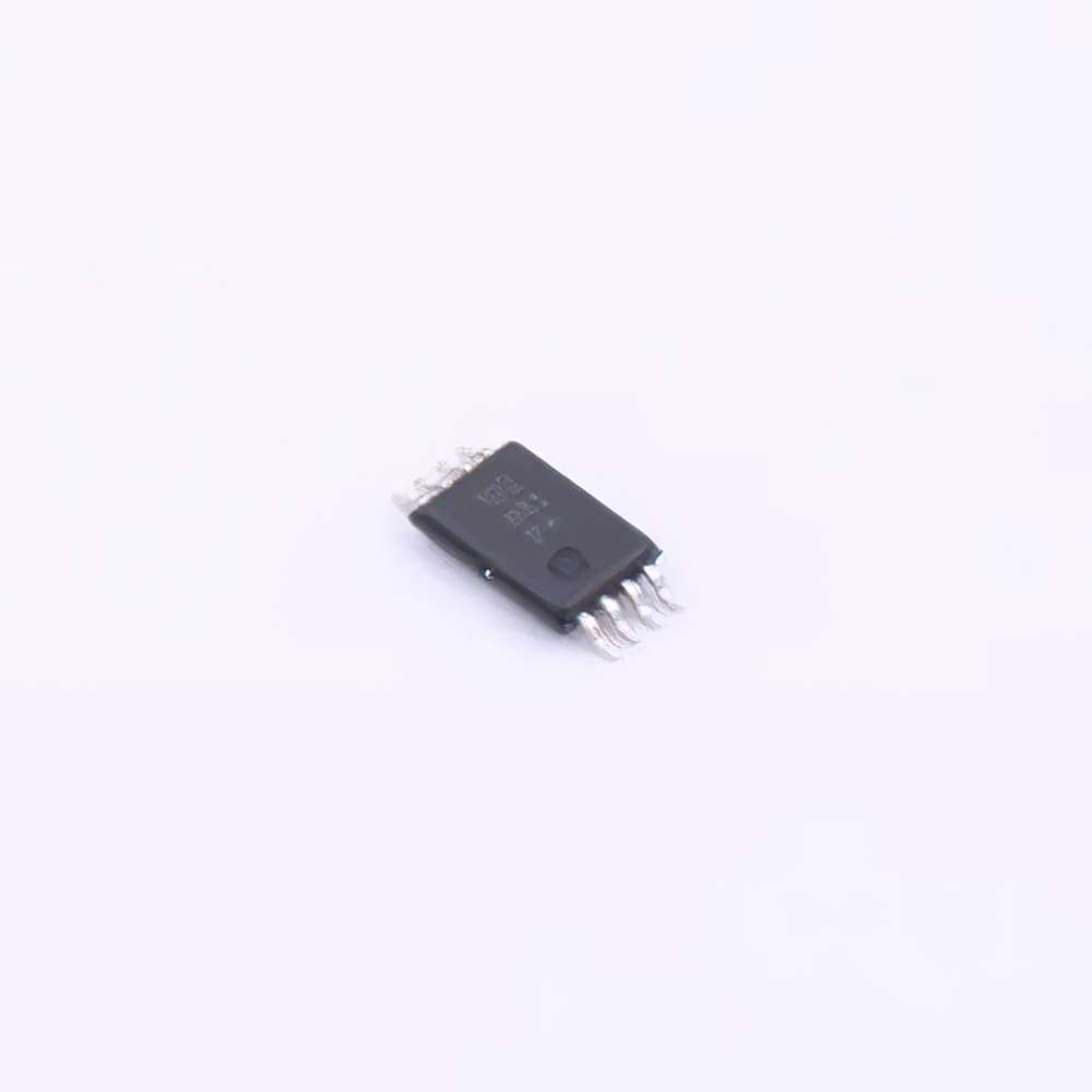
NB3V8312CFAR2G
12 LVCMOS/LVTTL
部品番号
NB3V8312CFAR2G
カテゴリー
RTC/Clock Chip > Clock Buffer, Driver
メーカー/ブランド
onsemi (Ansemi)
カプセル化
LQFP-32(7x7)
パッキング
taping
パッケージの数
2000
説明
The NB3V8312C is a high-performance, low-skew LVCMOS fan-out buffer that distributes 12 ultra-low-jitter clocks based on LVCMOS/LVTTL inputs up to 250 MHz. Twelve LVCMOS output pins drive 50Ω series or parallel terminated transmission lines. These outputs can also be disabled as high impedance (tri-state) via the OE input, or enabled when high. NB3V8312C provides an enable input, CLK_EN pin, which simultaneously enables the clock output, or disables it in a low state. Because this input is internally synchronized to the input clock and only changes when the input is low, there is no output glitch or runt pulse generation. Separate VDD core and VDDO output supplies allow the output buffer to operate at a supply voltage equal to VDD (VDD = VDDO) or lower. Dual-supply operation enables lower power consumption and output level compatibility compared to single-supply operation. The VDD core supply voltage can be set to 3.3 V, 2.5 V, or 1.8 V, and the VDDO output supply voltage can be set to 3.3 V, 2.5 V, or 1.8 V, but there is a constraint that VDD >/= VDDO.
リクエスト引用
必須フィールドをすべて入力し、送信をクリックしてください。12 時間以内に電子メールでご連絡いたします。何か問題がございましたら、メッセージを残すか、[email protected] まで電子メールを送信してください。 できるだけ早く対応させていただきます。
在庫あり 98466 PCS
連絡先
関連製品
1.8-V Programmable OmniClock Generator with Single-Ended (LVCMOS) and Differential (LVDS/HCSL) Outputs
onsemi (Ansemi)
のキーワード NB3V8312CFAR2G
NB3V8312CFAR2G 電子部品
NB3V8312CFAR2G 売上
NB3V8312CFAR2G サプライヤー
NB3V8312CFAR2G ディストリビュータ
NB3V8312CFAR2G データテーブル
NB3V8312CFAR2Gの写真
NB3V8312CFAR2G 価格
NB3V8312CFAR2G オファー
NB3V8312CFAR2G 最安値
NB3V8312CFAR2G 検索
NB3V8312CFAR2G を購入中
NB3V8312CFAR2G チップ