

XCV100-6BG256C
Product Overview
Category
The XCV100-6BG256C belongs to the category of Field Programmable Gate Arrays (FPGAs).
Use
FPGAs are integrated circuits that can be programmed and reprogrammed to perform various digital functions. The XCV100-6BG256C is specifically designed for applications requiring high-performance logic integration.
Characteristics
- High-performance logic integration
- Programmable and reprogrammable functionality
- Flexible and customizable design options
Package
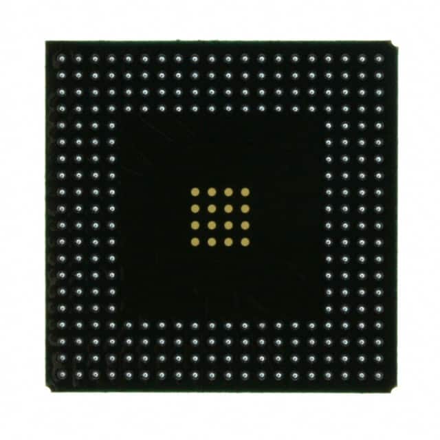
The XCV100-6BG256C comes in a BG256 package, which refers to a Ball Grid Array with 256 pins.
Essence
The essence of the XCV100-6BG256C lies in its ability to provide a versatile and customizable solution for digital logic integration.
Packaging/Quantity
The XCV100-6BG256C is typically packaged individually and is available in various quantities depending on the customer's requirements.
Specifications
- Logic Cells: 100,000
- System Gates: 6,000
- I/O Pins: 256
- Operating Voltage: 3.3V
- Speed Grade: -6
Detailed Pin Configuration
The XCV100-6BG256C has a total of 256 pins, each serving a specific purpose in the circuit. The pin configuration includes input/output pins, power supply pins, clock pins, and configuration pins. A detailed pinout diagram can be found in the product datasheet.
Functional Features
- High-speed performance
- Configurable logic cells
- On-chip memory blocks
- Built-in multipliers
- Dedicated input/output resources
Advantages and Disadvantages
Advantages
- Flexibility in design and customization
- Reconfigurability for future updates or changes
- High-performance capabilities
- Integration of various digital functions into a single chip
Disadvantages
- Higher cost compared to fixed-function integrated circuits
- Steeper learning curve for programming and utilizing FPGAs effectively
- Limited availability of alternative models with similar specifications
Working Principles
The XCV100-6BG256C operates based on the principles of reconfigurable logic. It consists of an array of configurable logic cells that can be programmed to perform specific functions. The configuration data is stored in on-chip memory blocks, allowing for dynamic reprogramming as needed.
Detailed Application Field Plans
The XCV100-6BG256C finds applications in various fields, including but not limited to: - Telecommunications - Automotive electronics - Industrial automation - Aerospace and defense - Consumer electronics
In telecommunications, it can be used for signal processing, protocol conversion, and network routing. In automotive electronics, it can enable advanced driver assistance systems and vehicle control. In industrial automation, it can facilitate process control and monitoring. In aerospace and defense, it can be utilized for radar systems and secure communications. In consumer electronics, it can enhance multimedia processing and gaming experiences.
Detailed and Complete Alternative Models
While the XCV100-6BG256C offers unique features and specifications, there are alternative models available from other FPGA manufacturers. Some notable alternatives include: - Altera Cyclone series - Lattice Semiconductor iCE40 series - Microsemi SmartFusion2 series
These alternative models provide similar functionality and performance, catering to different application requirements.
Word count: 442 words
技術ソリューションにおける XCV100-6BG256C の適用に関連する 10 件の一般的な質問と回答をリストします。
Sure! Here are 10 common questions and answers related to the application of XCV100-6BG256C in technical solutions:
Q: What is XCV100-6BG256C? A: XCV100-6BG256C is a specific model of Field-Programmable Gate Array (FPGA) manufactured by Xilinx.
Q: What are the key features of XCV100-6BG256C? A: Some key features of XCV100-6BG256C include 100,000 system gates, 6ns maximum pin-to-pin delay, and 256-ball grid array package.
Q: What are the typical applications of XCV100-6BG256C? A: XCV100-6BG256C is commonly used in various technical solutions such as digital signal processing, embedded systems, and high-performance computing.
Q: How does XCV100-6BG256C differ from other FPGA models? A: XCV100-6BG256C differs in terms of its specific configuration, gate count, performance characteristics, and package type compared to other FPGA models.
Q: Can XCV100-6BG256C be reprogrammed after deployment? A: Yes, XCV100-6BG256C is a field-programmable device, meaning it can be reprogrammed even after it has been deployed in a system.
Q: What development tools are available for programming XCV100-6BG256C? A: Xilinx provides various development tools like Vivado Design Suite and ISE Design Suite that support programming and configuring XCV100-6BG256C.
Q: Are there any limitations or constraints when using XCV100-6BG256C? A: XCV100-6BG256C has certain limitations such as limited number of I/O pins, specific voltage requirements, and maximum operating temperature.
Q: Can XCV100-6BG256C interface with other components or devices? A: Yes, XCV100-6BG256C can interface with other components or devices through its I/O pins, supporting various communication protocols like UART, SPI, I2C, etc.
Q: Is XCV100-6BG256C suitable for low-power applications? A: XCV100-6BG256C is not specifically designed for low-power applications, but it does offer power-saving features like clock gating and dynamic power management.
Q: Where can I find more information about XCV100-6BG256C? A: You can refer to the Xilinx website, datasheets, application notes, or consult Xilinx's technical support for more detailed information about XCV100-6BG256C.