

XCV100-5BG256C
Product Overview
Category
The XCV100-5BG256C belongs to the category of Field Programmable Gate Arrays (FPGAs).
Use
FPGAs are integrated circuits that can be programmed and reprogrammed to perform various digital functions. The XCV100-5BG256C is specifically designed for applications that require high-performance logic and signal processing capabilities.
Characteristics
- High-performance FPGA with advanced features
- Flexible and reprogrammable design
- Suitable for complex digital designs
- Offers high-speed data processing capabilities
- Provides a wide range of I/O options
Package
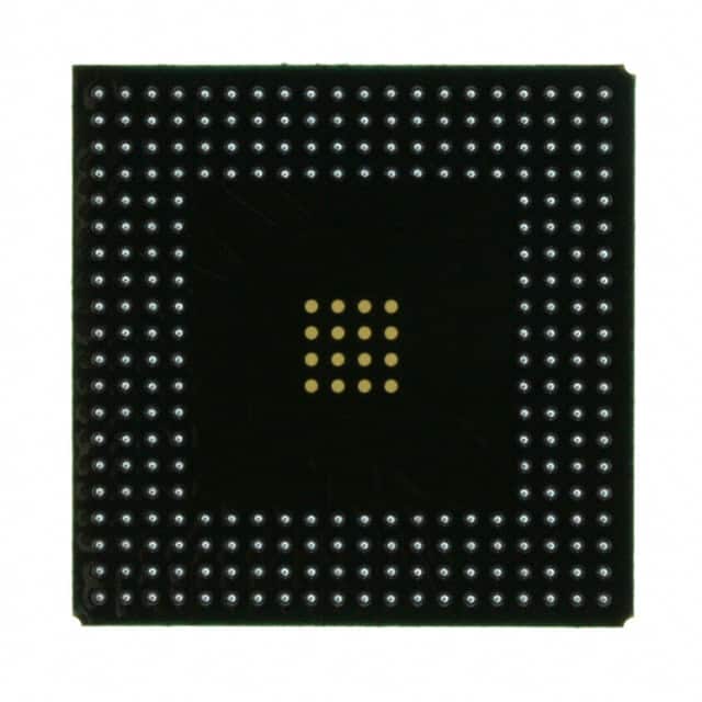
The XCV100-5BG256C comes in a 256-ball grid array (BGA) package, which provides a compact and reliable form factor for easy integration into electronic systems.
Essence
The essence of the XCV100-5BG256C lies in its ability to provide a customizable and versatile solution for digital circuit design and implementation.
Packaging/Quantity
The XCV100-5BG256C is typically packaged individually and is available in various quantities depending on the requirements of the customer or application.
Specifications
- Logic Cells: 100,000
- Flip-Flops: 50,000
- Block RAM: 2,560 Kbits
- DSP Slices: 80
- Maximum Frequency: 500 MHz
- Operating Voltage: 1.8V
- I/O Standards: LVCMOS, LVTTL, LVDS, etc.
- Package Type: BGA
- Package Pins: 256
Detailed Pin Configuration
The XCV100-5BG256C has a total of 256 pins arranged in a specific configuration. The pinout diagram and detailed pin descriptions can be found in the product datasheet.
Functional Features
- High-speed data processing capabilities
- Configurable logic cells for custom digital circuit implementation
- Dedicated DSP slices for efficient signal processing
- Flexible I/O options for interfacing with external devices
- On-chip memory blocks for data storage and retrieval
Advantages and Disadvantages
Advantages
- Versatile and reprogrammable design
- High-performance capabilities
- Wide range of I/O options
- Efficient signal processing capabilities
Disadvantages
- Relatively high power consumption compared to other programmable logic devices
- Steeper learning curve for beginners due to the complexity of FPGA programming
Working Principles
The XCV100-5BG256C operates based on the principles of configurable logic. It consists of a matrix of programmable logic cells that can be interconnected to implement various digital functions. The configuration of these logic cells is determined by the user's program, which is loaded onto the FPGA.
Detailed Application Field Plans
The XCV100-5BG256C finds applications in various fields, including: 1. Telecommunications: Used in base stations, network routers, and communication equipment. 2. Industrial Automation: Employed in control systems, robotics, and machine vision applications. 3. Aerospace and Defense: Utilized in radar systems, avionics, and secure communication systems. 4. Medical Devices: Integrated into imaging systems, patient monitoring devices, and diagnostic equipment. 5. Automotive: Applied in advanced driver-assistance systems (ADAS), infotainment systems, and engine control units.
Detailed and Complete Alternative Models
- XCV200-6FG256C: A higher-capacity FPGA with 200,000 logic cells and enhanced performance.
- XCV50-4PQ240I: A lower-cost FPGA with 50,000 logic cells and reduced power consumption.
- XCV400E-7FG680C: An FPGA with extended temperature range and 400,000 logic cells for rugged applications.
These alternative models offer different specifications and features to cater to diverse application requirements.
Word count: 511
技術ソリューションにおける XCV100-5BG256C の適用に関連する 10 件の一般的な質問と回答をリストします。
What is the maximum operating frequency of XCV100-5BG256C?
- The maximum operating frequency of XCV100-5BG256C is 100 MHz.What is the typical power consumption of XCV100-5BG256C?
- The typical power consumption of XCV100-5BG256C is 1.5W.Can XCV100-5BG256C be used in automotive applications?
- No, XCV100-5BG256C is not recommended for automotive applications due to its operating temperature range.What are the available I/O standards for XCV100-5BG256C?
- XCV100-5BG256C supports various I/O standards including LVCMOS, LVTTL, and HSTL.Is XCV100-5BG256C suitable for high-speed data processing?
- Yes, XCV100-5BG256C is suitable for high-speed data processing applications.What is the maximum number of logic cells in XCV100-5BG256C?
- XCV100-5BG256C has a maximum of 10,000 logic cells.Can XCV100-5BG256C be reprogrammed multiple times?
- Yes, XCV100-5BG256C is reprogrammable and can be reconfigured multiple times.Does XCV100-5BG256C support JTAG boundary scan testing?
- Yes, XCV100-5BG256C supports JTAG boundary scan testing for debugging and testing purposes.What is the voltage supply range for XCV100-5BG256C?
- XCV100-5BG256C operates with a voltage supply range of 3.3V ± 0.3V.Can XCV100-5BG256C interface with external memory devices?
- Yes, XCV100-5BG256C can interface with external memory devices using its dedicated memory interfaces.