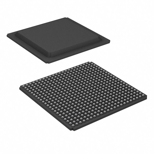
XC7S100-L1FGGA484I
Product Overview
Category
The XC7S100-L1FGGA484I belongs to the category of Field-Programmable Gate Arrays (FPGAs).
Use
FPGAs are integrated circuits that can be programmed and reprogrammed to perform various digital functions. The XC7S100-L1FGGA484I is specifically designed for high-performance applications that require complex logic functions.
Characteristics
- High-performance FPGA with advanced features
- Large number of programmable logic cells
- Flexible and reconfigurable design
- Low power consumption
- High-speed data processing capabilities
Package
The XC7S100-L1FGGA484I comes in a Fine-Pitch Ball Grid Array (FGGA) package, which provides a compact form factor and efficient heat dissipation.
Essence
The essence of the XC7S100-L1FGGA484I lies in its ability to provide a customizable hardware platform for implementing complex digital designs.
Packaging/Quantity
The XC7S100-L1FGGA484I is typically sold in reels or trays, with each reel or tray containing a specific quantity of FPGAs.
Specifications
- Logic Cells: 100,000
- Block RAM: 4,860 Kbits
- DSP Slices: 240
- Maximum Operating Frequency: 550 MHz
- I/O Pins: 484
- Voltage Range: 1.2V - 3.3V
- Operating Temperature Range: -40°C to 100°C
Detailed Pin Configuration
The XC7S100-L1FGGA484I has 484 I/O pins, which are used for input and output connections. These pins are arranged in a specific configuration to facilitate easy integration into electronic systems. For a detailed pin configuration diagram, please refer to the datasheet provided by the manufacturer.
Functional Features
- High-speed data processing: The XC7S100-L1FGGA484I offers fast data processing capabilities, making it suitable for applications that require real-time data handling.
- Reconfigurability: The FPGA can be reprogrammed to adapt to changing requirements, allowing for flexibility in system design.
- Large logic capacity: With 100,000 logic cells, the XC7S100-L1FGGA484I can accommodate complex digital designs.
- Low power consumption: The FPGA is designed to operate efficiently with low power consumption, making it suitable for battery-powered devices.
Advantages and Disadvantages
Advantages
- Flexibility in design due to reprogrammability
- High-performance capabilities
- Large logic capacity for complex designs
- Low power consumption for energy-efficient operation
Disadvantages
- Higher cost compared to fixed-function integrated circuits
- Steeper learning curve for programming and utilizing FPGAs effectively
Working Principles
FPGAs like the XC7S100-L1FGGA484I consist of an array of configurable logic blocks interconnected through programmable interconnects. These logic blocks can be programmed to implement various digital functions, such as arithmetic operations, memory storage, and control logic. The configuration of the FPGA is stored in non-volatile memory and can be modified using specialized software tools.
Detailed Application Field Plans
The XC7S100-L1FGGA484I finds applications in a wide range of industries and fields, including:
- Telecommunications: Used in high-speed data communication systems, network routers, and switches.
- Aerospace and Defense: Employed in radar systems, avionics, and military communication equipment.
- Industrial Automation: Utilized in programmable logic controllers (PLCs), motor control systems, and robotics.
- Medical Devices: Integrated into medical imaging equipment, patient monitoring systems, and diagnostic devices.
- Automotive: Used in advanced driver-assistance systems (ADAS), infotainment systems, and engine control units.
Detailed and Complete Alternative Models
- XC7S50-L1FGGA484I: A lower-capacity version of the XC7S100-L1FGGA484I with 50,000 logic cells.
- XC7S200-L1FGGA484I: A higher-capacity version of the XC7S100-L1FGGA484I with 200,000 logic cells.
- XC7S400-L1FGGA484I: An even higher-capacity version of the XC7S100-L1FGGA484I with 400,000 logic cells.
These alternative models provide options for different design requirements, allowing users to choose the FPGA that best suits their specific needs.
In conclusion, the XC7S100-L1FGGA484I is a high-performance FPGA that offers flexibility, reconfigurability, and large logic capacity. It finds applications in various industries and can be used in diverse digital design projects.
技術ソリューションにおける XC7S100-L1FGGA484I の適用に関連する 10 件の一般的な質問と回答をリストします。
Sure! Here are 10 common questions and answers related to the application of XC7S100-L1FGGA484I in technical solutions:
Q1: What is XC7S100-L1FGGA484I? A1: XC7S100-L1FGGA484I is a specific model of Xilinx Spartan-7 FPGA (Field Programmable Gate Array) with 100K logic cells, available in a FGGA484 package.
Q2: What are the key features of XC7S100-L1FGGA484I? A2: Some key features of XC7S100-L1FGGA484I include high-performance programmable logic, integrated memory blocks, DSP slices, and support for various I/O standards.
Q3: What are the typical applications of XC7S100-L1FGGA484I? A3: XC7S100-L1FGGA484I can be used in a wide range of applications such as industrial automation, automotive electronics, telecommunications, medical devices, and more.
Q4: How can XC7S100-L1FGGA484I be programmed? A4: XC7S100-L1FGGA484I can be programmed using Xilinx's Vivado Design Suite or other compatible programming tools.
Q5: What is the power supply requirement for XC7S100-L1FGGA484I? A5: XC7S100-L1FGGA484I typically requires a power supply voltage of 1.2V, but it also supports other voltage levels for different I/O standards.
Q6: Can XC7S100-L1FGGA484I interface with external devices? A6: Yes, XC7S100-L1FGGA484I has multiple I/O banks that can be configured to interface with various external devices such as sensors, displays, memory, and communication interfaces.
Q7: What is the maximum operating frequency of XC7S100-L1FGGA484I? A7: The maximum operating frequency of XC7S100-L1FGGA484I depends on the design and implementation, but it can typically achieve frequencies in the range of several hundred megahertz (MHz) to a few gigahertz (GHz).
Q8: Can XC7S100-L1FGGA484I be used for real-time signal processing? A8: Yes, XC7S100-L1FGGA484I's integrated DSP slices and high-performance programmable logic make it suitable for real-time signal processing applications.
Q9: Does XC7S100-L1FGGA484I support secure boot and encryption? A9: Yes, XC7S100-L1FGGA484I supports features like secure boot and bitstream encryption, which help protect the intellectual property and ensure secure operation.
Q10: Are there any development boards available for XC7S100-L1FGGA484I? A10: Yes, Xilinx offers various development boards that are compatible with XC7S100-L1FGGA484I, allowing users to prototype and develop their designs efficiently.
Please note that these questions and answers are general and may vary depending on specific requirements and use cases.


