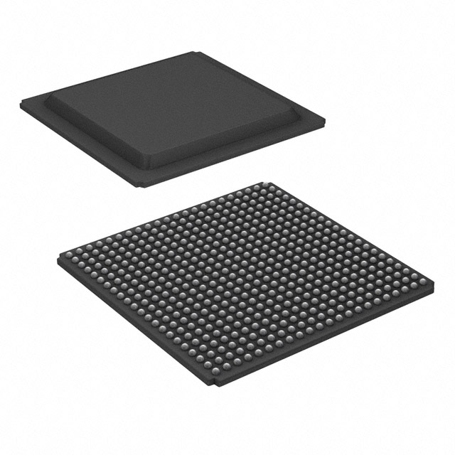
XC7A100T-1FGG484I
Product Overview
Category
XC7A100T-1FGG484I belongs to the category of Field Programmable Gate Arrays (FPGAs).
Use
This product is primarily used in digital circuit design and implementation. FPGAs offer a flexible and customizable solution for various applications, including telecommunications, automotive, aerospace, and consumer electronics.
Characteristics
XC7A100T-1FGG484I is known for its high performance, low power consumption, and reconfigurability. It provides a cost-effective solution for complex digital designs that require rapid prototyping and frequent design iterations.
Package
The XC7A100T-1FGG484I FPGA comes in a 484-pin Fine-Pitch Ball Grid Array (FBGA) package.
Essence
The essence of XC7A100T-1FGG484I lies in its ability to implement complex digital circuits with high speed and efficiency. Its reprogrammable nature allows for quick design changes without the need for physical hardware modifications.
Packaging/Quantity
XC7A100T-1FGG484I is typically sold individually or in small quantities, depending on the supplier's packaging options.
Specifications
- Logic Cells: 101,440
- Flip-Flops: 63,800
- Block RAM: 4,860 Kb
- DSP Slices: 240
- Maximum Operating Frequency: 600 MHz
- I/O Pins: 332
- Voltage Range: 0.95V - 1.05V
Detailed Pin Configuration
For a detailed pin configuration diagram of XC7A100T-1FGG484I, please refer to the manufacturer's datasheet or documentation.
Functional Features
XC7A100T-1FGG484I offers several functional features that make it a versatile FPGA for various applications:
- High Logic Capacity: With over 100,000 logic cells, it can accommodate complex digital designs.
- Reconfigurability: The ability to modify the design without changing the physical hardware allows for rapid prototyping and design iterations.
- Low Power Consumption: XC7A100T-1FGG484I is designed to operate efficiently, minimizing power consumption.
- High-Speed Performance: With a maximum operating frequency of 600 MHz, it can handle demanding applications that require fast data processing.
- Ample I/O Pins: The FPGA provides 332 I/O pins, enabling seamless integration with external devices.
Advantages and Disadvantages
Advantages
- Flexibility in design modifications
- Rapid prototyping capabilities
- High logic capacity
- Low power consumption
- Wide range of applications
Disadvantages
- Steep learning curve for beginners
- Higher cost compared to other programmable logic devices
- Limited availability of alternative models
Working Principles
XC7A100T-1FGG484I operates based on the principles of reconfigurable computing. It consists of an array of configurable logic blocks interconnected through programmable routing resources. These logic blocks can be programmed to implement desired digital circuits by configuring their internal look-up tables, flip-flops, and interconnections.
The configuration of XC7A100T-1FGG484I is stored in non-volatile memory, allowing it to retain the design even after power-off. During operation, the FPGA executes the configured circuit by routing signals through the programmable interconnects and performing logical operations within the logic blocks.
Detailed Application Field Plans
XC7A100T-1FGG484I finds applications in various fields, including:
- Telecommunications: Used in base stations, routers, and network switches for high-speed data processing and protocol handling.
- Automotive: Employed in advanced driver-assistance systems (ADAS), infotainment systems, and engine control units (ECUs) for efficient data processing and control.
- Aerospace: Utilized in satellite communication systems, avionics, and radar systems for reliable and high-performance signal processing.
- Consumer Electronics: Integrated into smart TVs, gaming consoles, and wearable devices to enable complex functionalities and multimedia processing.
Detailed and Complete Alternative Models
While XC7A100T-1FGG484I is a popular FPGA model, there are alternative models available from various manufacturers that offer similar capabilities. Some notable alternatives include:
- Intel Cyclone V GX: Offers comparable logic capacity and performance with a different architecture.
- Lattice ECP5: Provides low-power consumption and high-speed performance for cost-sensitive applications.
- Microsemi SmartFusion2: Combines FPGA fabric with a microcontroller subsystem for embedded system designs.
These alternative models can be considered based on specific project requirements and design constraints.
In conclusion, XC7A100T-1FGG484I is a versatile FPGA that offers high performance, re
技術ソリューションにおける XC7A100T-1FGG484I の適用に関連する 10 件の一般的な質問と回答をリストします。
Sure! Here are 10 common questions and answers related to the application of XC7A100T-1FGG484I in technical solutions:
Q1: What is XC7A100T-1FGG484I? A1: XC7A100T-1FGG484I is a field-programmable gate array (FPGA) manufactured by Xilinx. It is part of the Artix-7 family and has 100,000 logic cells.
Q2: What are some typical applications of XC7A100T-1FGG484I? A2: XC7A100T-1FGG484I is commonly used in various technical solutions such as industrial automation, telecommunications, automotive electronics, medical devices, and aerospace systems.
Q3: What are the key features of XC7A100T-1FGG484I? A3: Some key features of XC7A100T-1FGG484I include high-performance programmable logic, integrated memory blocks, DSP slices for signal processing, multiple I/O standards, and low power consumption.
Q4: How can XC7A100T-1FGG484I be programmed? A4: XC7A100T-1FGG484I can be programmed using Xilinx's Vivado Design Suite, which provides a graphical interface for designing, simulating, and programming the FPGA.
Q5: Can XC7A100T-1FGG484I be used for real-time applications? A5: Yes, XC7A100T-1FGG484I can be used for real-time applications due to its high-speed performance and ability to handle complex algorithms efficiently.
Q6: What are the advantages of using XC7A100T-1FGG484I in technical solutions? A6: Some advantages of using XC7A100T-1FGG484I include its flexibility, reconfigurability, high processing power, low latency, and ability to interface with various peripherals.
Q7: Can XC7A100T-1FGG484I be used in safety-critical applications? A7: Yes, XC7A100T-1FGG484I can be used in safety-critical applications as long as proper design practices, redundancy, and fault-tolerant mechanisms are implemented.
Q8: What is the maximum operating frequency of XC7A100T-1FGG484I? A8: The maximum operating frequency of XC7A100T-1FGG484I depends on the specific design and implementation but can typically reach several hundred megahertz (MHz) or even gigahertz (GHz).
Q9: Can XC7A100T-1FGG484I interface with other components or devices? A9: Yes, XC7A100T-1FGG484I supports various I/O standards and can interface with other components or devices such as sensors, actuators, memory modules, communication interfaces, and more.
Q10: Are there any development boards available for XC7A100T-1FGG484I? A10: Yes, Xilinx provides development boards like the Arty A7-100T, which feature XC7A100T-1FGG484I, allowing users to prototype and develop their designs easily.
Please note that these answers are general and may vary depending on specific requirements and implementations.


