

XC6SLX150T-2FGG900I
Product Overview
Category
XC6SLX150T-2FGG900I belongs to the category of Field Programmable Gate Arrays (FPGAs).
Use
This product is primarily used in digital logic circuits and electronic systems design. FPGAs provide a flexible and customizable solution for implementing complex digital designs.
Characteristics
- High-performance FPGA with advanced features
- Large capacity and high-speed processing capabilities
- Configurable logic blocks and programmable interconnects
- Support for various communication protocols and interfaces
- Flexible and reprogrammable design
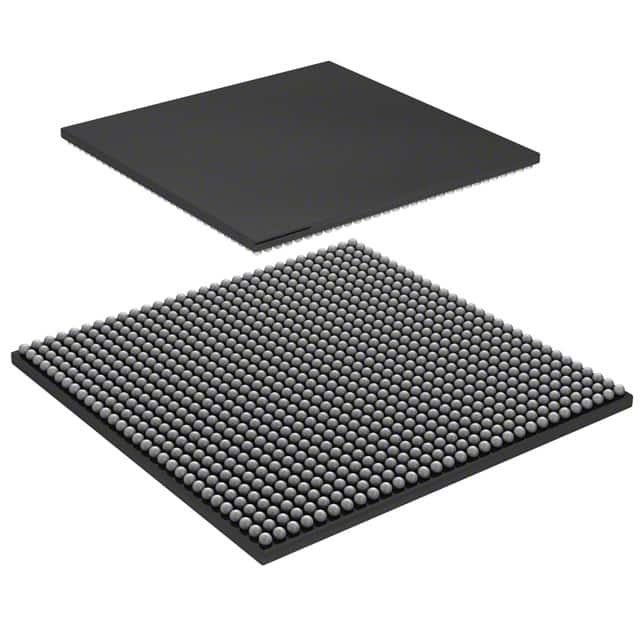
Package
XC6SLX150T-2FGG900I is available in a specific package type, which ensures proper protection and compatibility with other components in the system.
Essence
The essence of XC6SLX150T-2FGG900I lies in its ability to provide a versatile platform for implementing complex digital designs. It offers a high level of customization and adaptability, making it suitable for a wide range of applications.
Packaging/Quantity
XC6SLX150T-2FGG900I is typically packaged individually and is available in varying quantities depending on the manufacturer or distributor.
Specifications
- FPGA Family: Spartan-6
- Logic Cells: 147,443
- Flip-Flops: 92,160
- Block RAM: 4,860 Kbits
- DSP Slices: 360
- Maximum Frequency: 550 MHz
- Operating Voltage: 1.2V
- Package Type: FG900
Detailed Pin Configuration
The detailed pin configuration of XC6SLX150T-2FGG900I can be found in the product datasheet provided by the manufacturer. It includes information about the pin names, functions, and electrical characteristics.
Functional Features
XC6SLX150T-2FGG900I offers several functional features that enhance its performance and usability:
Configurable Logic Blocks (CLBs): These blocks provide the building blocks for implementing digital logic circuits. They consist of Look-Up Tables (LUTs), flip-flops, and multiplexers.
Programmable Interconnects: The interconnect structure allows for flexible routing of signals between different logic elements, enabling complex designs to be implemented efficiently.
Embedded Memory: XC6SLX150T-2FGG900I includes embedded Block RAM (BRAM) resources, which can be used for data storage or as FIFO buffers.
High-Speed Serial Transceivers: This FPGA supports high-speed serial communication protocols such as PCIe, SATA, and Ethernet, enabling fast data transfer rates.
Advantages and Disadvantages
Advantages
- High-performance FPGA with large capacity
- Flexible and reprogrammable design
- Support for various communication protocols
- Cost-effective solution compared to custom ASIC designs
Disadvantages
- Steeper learning curve compared to traditional digital logic design
- Limited availability of alternative models with similar specifications
- Higher power consumption compared to specialized ASICs in some cases
Working Principles
XC6SLX150T-2FGG900I operates based on the principles of configurable logic and programmable interconnects. The FPGA is programmed using a Hardware Description Language (HDL) such as VHDL or Verilog, which describes the desired digital circuit functionality. The programming file is then loaded onto the FPGA, configuring the logic elements and interconnects accordingly. Once programmed, the FPGA executes the desired digital circuit operations.
Detailed Application Field Plans
XC6SLX150T-2FGG900I finds applications in various fields, including:
Telecommunications: Used in base stations, routers, and network switches for high-speed data processing and communication.
Aerospace and Defense: Employed in radar systems, avionics, and military communication equipment for their high-performance and reconfigurable nature.
Industrial Automation: Utilized in control systems, motor drives, and robotics for real-time processing and control.
Medical Devices: Integrated into medical imaging systems, patient monitoring devices, and laboratory equipment for their processing capabilities.
Detailed and Complete Alternative Models
While XC6SLX150T-2FGG900I offers unique specifications and features, there are alternative FPGA models available from different manufacturers that can be considered based on specific requirements. Some notable alternatives include:
- Xilinx Virtex-7 Series
- Intel (Altera) Cyclone V Series
- Lattice Semiconductor ECP5 Series
- Microchip PolarFire Series
These alternative models provide a range of options with varying capacities, performance levels, and pricing to suit different application needs.
In conclusion, XC6SLX150T-2FGG900I is a high-performance FPGA belonging to the Spartan-6 family. It offers flexibility, customization, and advanced features
技術ソリューションにおける XC6SLX150T-2FGG900I の適用に関連する 10 件の一般的な質問と回答をリストします。
Sure! Here are 10 common questions and answers related to the application of XC6SLX150T-2FGG900I in technical solutions:
Q: What is XC6SLX150T-2FGG900I? A: XC6SLX150T-2FGG900I is a field-programmable gate array (FPGA) from Xilinx, which offers high-performance processing capabilities for various technical applications.
Q: What are the key features of XC6SLX150T-2FGG900I? A: Some key features include a large number of logic cells, high-speed serial transceivers, embedded memory blocks, DSP slices, and support for various communication protocols.
Q: What technical solutions can XC6SLX150T-2FGG900I be used for? A: XC6SLX150T-2FGG900I can be used in a wide range of applications such as telecommunications, aerospace, defense, industrial automation, medical devices, and scientific research.
Q: How can XC6SLX150T-2FGG900I enhance system performance? A: By leveraging its high-speed processing capabilities, parallel computing architecture, and ability to implement complex algorithms, XC6SLX150T-2FGG900I can significantly improve system performance.
Q: Can XC6SLX150T-2FGG900I be reprogrammed after deployment? A: Yes, XC6SLX150T-2FGG900I is a field-programmable device, meaning it can be reconfigured or reprogrammed even after it has been deployed in a system.
Q: What development tools are available for programming XC6SLX150T-2FGG900I? A: Xilinx provides a suite of development tools, including Vivado Design Suite and ISE Design Suite, which offer comprehensive features for designing, simulating, and programming XC6SLX150T-2FGG900I.
Q: Can XC6SLX150T-2FGG900I interface with other components or devices? A: Yes, XC6SLX150T-2FGG900I supports various communication protocols such as PCIe, Ethernet, USB, SPI, I2C, and UART, allowing it to interface with a wide range of components and devices.
Q: What are the power requirements for XC6SLX150T-2FGG900I? A: XC6SLX150T-2FGG900I typically operates at a voltage range of 1.14V to 1.26V, with power consumption varying depending on the application and configuration.
Q: Are there any limitations or considerations when using XC6SLX150T-2FGG900I? A: Some considerations include thermal management due to high power dissipation, potential signal integrity issues at high speeds, and the need for expertise in FPGA design and programming.
Q: Where can I find additional resources or support for XC6SLX150T-2FGG900I? A: Xilinx provides extensive documentation, user guides, application notes, and online forums where you can find additional resources and seek support for XC6SLX150T-2FGG900I.