

XC4005XL-3PQ100C
Product Overview
Category
The XC4005XL-3PQ100C belongs to the category of Field Programmable Gate Arrays (FPGAs).
Use
FPGAs are integrated circuits that can be programmed and reprogrammed to perform various digital functions. The XC4005XL-3PQ100C is specifically designed for applications requiring high-performance logic integration.
Characteristics
- High-performance logic integration
- Programmable and reprogrammable functionality
- Flexible and customizable design options
Package
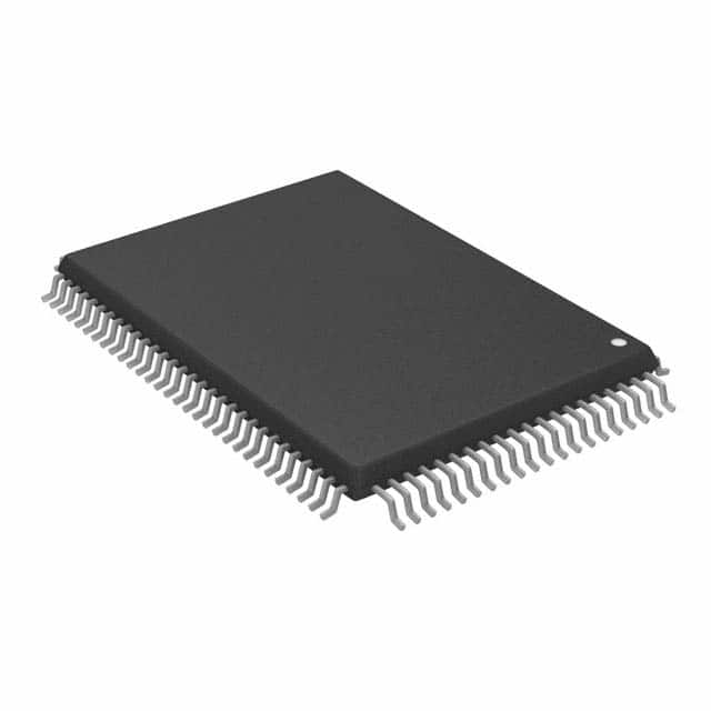
The XC4005XL-3PQ100C comes in a PQ100 package, which refers to a plastic quad flat pack with 100 pins.
Essence
The essence of the XC4005XL-3PQ100C lies in its ability to provide a versatile and configurable solution for complex digital designs.
Packaging/Quantity
The XC4005XL-3PQ100C is typically packaged in reels or trays, with each reel or tray containing a specific quantity of units. The exact packaging and quantity may vary depending on the supplier.
Specifications
- Logic Cells: 4000
- Maximum Frequency: 100 MHz
- Operating Voltage: 3.3V
- I/O Pins: 100
- Programmable Logic Blocks: 128
- RAM Bits: 64,000
- Flip-Flops: 4,000
- Configuration Memory: 1,024 bits
Detailed Pin Configuration
The XC4005XL-3PQ100C has a total of 100 pins, each serving a specific purpose in the overall functionality of the FPGA. The pin configuration includes input/output pins, power supply pins, clock pins, and configuration pins. A detailed pinout diagram can be found in the datasheet provided by the manufacturer.
Functional Features
- High-performance logic integration allows for complex digital designs.
- Programmable and reprogrammable functionality enables flexibility in design iterations.
- Configurable I/O pins provide versatility in interfacing with external devices.
- On-chip memory resources facilitate efficient data storage and retrieval.
- Built-in clock management circuitry ensures precise timing control.
Advantages
- Versatile and customizable design options cater to a wide range of applications.
- High-performance capabilities enable the implementation of complex algorithms.
- Reprogrammability allows for easy updates and modifications without hardware changes.
- Compact form factor saves space and reduces overall system complexity.
- Cost-effective solution compared to custom ASIC designs.
Disadvantages
- Limited resources compared to larger FPGAs, which may restrict the complexity of designs.
- Higher power consumption compared to dedicated application-specific integrated circuits (ASICs).
- Steeper learning curve for programming and utilizing the full potential of FPGAs.
- Susceptible to configuration errors that can lead to functional issues.
Working Principles
The XC4005XL-3PQ100C operates based on the principles of configurable logic. It consists of programmable logic blocks, interconnect resources, and input/output elements. The programmable logic blocks can be configured to implement various logical functions, while the interconnect resources allow for the routing of signals between different blocks. The input/output elements provide the interface between the FPGA and external devices.
Detailed Application Field Plans
The XC4005XL-3PQ100C finds applications in various fields, including:
- Communications: Used in networking equipment, routers, and switches for high-speed data processing.
- Industrial Automation: Employed in control systems, robotics, and machine vision applications.
- Aerospace and Defense: Utilized in radar systems, avionics, and secure communication systems.
- Automotive: Integrated into advanced driver-assistance systems (ADAS) and infotainment systems.
- Medical: Applied in medical imaging, patient monitoring, and diagnostic equipment.
Detailed and Complete Alternative Models
- XC4006E-4PQ160C: Similar to the XC4005XL-3PQ100C but with enhanced logic capacity and more I/O pins.
- XC4010E-3PQ160C: Offers increased logic cells and I/O pins compared to the XC4005XL-3PQ100C.
- XC4028EX-3HQ240C: Provides higher performance and larger capacity for demanding applications.
- XC4036EX-4HQ240C: Suitable for complex designs requiring a greater number of logic cells and I/O pins.
- XC4062XLA-4HQ240C: Offers advanced features and expanded resources for highly sophisticated designs.
These alternative models provide varying levels of performance, capacity, and functionality to cater to different project requirements.
Word count: 605 words
技術ソリューションにおける XC4005XL-3PQ100C の適用に関連する 10 件の一般的な質問と回答をリストします。
Sure! Here are 10 common questions and answers related to the application of XC4005XL-3PQ100C in technical solutions:
Question: What is XC4005XL-3PQ100C?
Answer: XC4005XL-3PQ100C is a specific model of Xilinx FPGA (Field-Programmable Gate Array) used for implementing digital logic circuits.Question: What are the key features of XC4005XL-3PQ100C?
Answer: Some key features of XC4005XL-3PQ100C include 4000 logic cells, 64 I/O pins, 36Kbits of RAM, and support for various communication protocols.Question: What are the typical applications of XC4005XL-3PQ100C?
Answer: XC4005XL-3PQ100C is commonly used in applications such as industrial control systems, automotive electronics, telecommunications, and consumer electronics.Question: How do I program XC4005XL-3PQ100C?
Answer: XC4005XL-3PQ100C can be programmed using Xilinx's programming tools like Vivado or ISE Design Suite. You can write your design in a hardware description language (HDL) like VHDL or Verilog and then generate a bitstream file to program the FPGA.Question: Can XC4005XL-3PQ100C be reprogrammed?
Answer: Yes, XC4005XL-3PQ100C is a reprogrammable FPGA, which means you can change the functionality by reprogramming it with a new bitstream file.Question: What voltage levels does XC4005XL-3PQ100C support?
Answer: XC4005XL-3PQ100C supports both 3.3V and 5V voltage levels, making it compatible with a wide range of digital systems.Question: Can XC4005XL-3PQ100C interface with other components or devices?
Answer: Yes, XC4005XL-3PQ100C can interface with various components and devices through its I/O pins, supporting protocols like SPI, I2C, UART, and more.Question: What is the power consumption of XC4005XL-3PQ100C?
Answer: The power consumption of XC4005XL-3PQ100C depends on the design and utilization of the FPGA. It is recommended to refer to the datasheet for detailed power specifications.Question: Are there any limitations or constraints when using XC4005XL-3PQ100C?
Answer: XC4005XL-3PQ100C has certain limitations such as limited logic resources, I/O pins, and memory capacity. It's important to consider these constraints while designing your solution.Question: Where can I find additional resources and support for XC4005XL-3PQ100C?
Answer: You can find additional resources, documentation, and support for XC4005XL-3PQ100C on Xilinx's official website, including user guides, application notes, and forums for community discussions.