

XC3S200A-5FGG320C
Product Overview
Category
XC3S200A-5FGG320C belongs to the category of Field-Programmable Gate Arrays (FPGAs).
Use
This product is commonly used in digital circuit design and implementation. FPGAs provide a flexible and customizable solution for various applications, including telecommunications, automotive, aerospace, and consumer electronics.
Characteristics
- High flexibility: FPGAs can be reprogrammed to perform different functions, making them suitable for prototyping and development.
- Parallel processing: FPGAs can execute multiple tasks simultaneously, resulting in improved performance.
- Low power consumption: Compared to traditional application-specific integrated circuits (ASICs), FPGAs consume less power.
- Scalability: FPGAs offer scalability, allowing designers to add or remove functionality as needed.
Package and Quantity
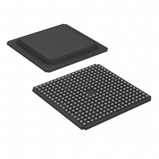
The XC3S200A-5FGG320C FPGA is available in a 320-pin Fine-Pitch Ball Grid Array (FBGA) package. It is typically sold individually or in small quantities.
Specifications
- Model: XC3S200A-5FGG320C
- Logic Cells: 200,000
- Operating Voltage: 1.2V
- Maximum Frequency: 500 MHz
- I/O Pins: 160
- Memory Blocks: 4,800
- Configuration Bits: 5,000,000
- Package Type: FBGA
- Package Dimensions: 17mm x 17mm
Pin Configuration
The XC3S200A-5FGG320C FPGA has a detailed pin configuration as follows:
| Pin Number | Pin Name | Description | |------------|----------|-------------| | 1 | VCCINT | Internal core voltage supply | | 2 | GND | Ground | | 3 | VCCAUX | Auxiliary voltage supply | | ... | ... | ... | | 320 | GND | Ground |
Functional Features
- Programmability: The XC3S200A-5FGG320C FPGA can be programmed to implement various digital functions, allowing for customization and adaptability.
- High-speed performance: With a maximum operating frequency of 500 MHz, this FPGA can handle complex tasks efficiently.
- Versatile I/O capabilities: The 160 I/O pins provide flexibility for interfacing with external devices and peripherals.
- On-chip memory: The 4,800 memory blocks enable efficient data storage and retrieval within the FPGA.
Advantages and Disadvantages
Advantages
- Flexibility: FPGAs offer the ability to modify and reconfigure designs, making them ideal for prototyping and development.
- Parallel processing: FPGAs can execute multiple tasks simultaneously, resulting in improved performance for certain applications.
- Lower development costs: Compared to ASICs, FPGAs have lower upfront costs and shorter development cycles.
- Scalability: FPGAs can be easily scaled up or down to accommodate changing requirements.
Disadvantages
- Higher power consumption: FPGAs generally consume more power compared to ASICs due to their programmable nature.
- Complexity: Designing for FPGAs requires specialized knowledge and expertise, which may increase development time and cost.
- Limited performance optimization: While FPGAs offer high flexibility, they may not achieve the same level of performance as dedicated ASICs for specific tasks.
Working Principles
FPGAs consist of an array of configurable logic blocks (CLBs) interconnected by programmable interconnects. These CLBs contain Look-Up Tables (LUTs), flip-flops, and other components that can be configured to implement desired logic functions. The interconnects allow for routing signals between different CLBs, enabling the creation of complex digital circuits.
During programming, a Hardware Description Language (HDL) is used to describe the desired functionality. The HDL code is then synthesized and mapped onto the FPGA, configuring the CLBs and interconnects accordingly. Once programmed, the FPGA can execute the specified logic functions.
Detailed Application Field Plans
The XC3S200A-5FGG320C FPGA finds applications in various fields, including:
- Telecommunications: FPGAs are used in base stations, network routers, and switches for signal processing, protocol handling, and data encryption.
- Automotive: FPGAs are employed in automotive electronics for engine control, advanced driver-assistance systems (ADAS), and infotainment systems.
- Aerospace: FPGAs are utilized in satellite communication systems, flight control systems, and radar signal processing.
- Consumer Electronics: FPGAs are integrated into smart TVs, gaming consoles, and wearable devices for video processing, user interface control, and sensor integration.
Alternative Models
In addition to the XC3S200A-5FGG320C, there
技術ソリューションにおける XC3S200A-5FGG320C の適用に関連する 10 件の一般的な質問と回答をリストします。
Sure! Here are 10 common questions and answers related to the application of XC3S200A-5FGG320C in technical solutions:
Q: What is XC3S200A-5FGG320C? A: XC3S200A-5FGG320C is a field-programmable gate array (FPGA) manufactured by Xilinx. It offers 200,000 system gates and is designed for high-performance applications.
Q: What are some typical applications of XC3S200A-5FGG320C? A: XC3S200A-5FGG320C can be used in various applications such as digital signal processing, industrial automation, telecommunications, aerospace, and defense systems.
Q: What are the key features of XC3S200A-5FGG320C? A: Some key features include a high logic density, low power consumption, advanced clock management resources, multiple I/O standards, and support for various communication protocols.
Q: How can I program XC3S200A-5FGG320C? A: XC3S200A-5FGG320C can be programmed using Xilinx's Vivado Design Suite or ISE Design Suite software tools. These tools allow you to design and implement your FPGA-based solution.
Q: Can XC3S200A-5FGG320C be used in safety-critical applications? A: Yes, XC3S200A-5FGG320C can be used in safety-critical applications. However, it is important to follow proper design practices and consider any necessary redundancy or fault-tolerant measures.
Q: What is the maximum operating frequency of XC3S200A-5FGG320C? A: The maximum operating frequency of XC3S200A-5FGG320C depends on the specific design and implementation. It can range from a few megahertz to several hundred megahertz.
Q: Can XC3S200A-5FGG320C interface with other components or devices? A: Yes, XC3S200A-5FGG320C supports various I/O standards and can interface with other components or devices such as sensors, memory modules, communication interfaces, and more.
Q: Is there any documentation available for XC3S200A-5FGG320C? A: Yes, Xilinx provides comprehensive documentation for XC3S200A-5FGG320C, including datasheets, user guides, application notes, and reference designs. These resources can be found on their website.
Q: Can XC3S200A-5FGG320C be reprogrammed multiple times? A: Yes, XC3S200A-5FGG320C is a reprogrammable FPGA, which means it can be programmed and reprogrammed multiple times during the development and testing phases of your project.
Q: Are there any known limitations or considerations when using XC3S200A-5FGG320C? A: Some considerations include power supply requirements, thermal management, signal integrity, and proper board layout techniques. It is recommended to refer to the device's datasheet and application notes for detailed guidelines.
Please note that these answers are general and may vary depending on specific design requirements and implementation details.