

XC2VP4-6FGG456I
Product Overview
- Category: Integrated Circuit (IC)
- Use: Programmable Logic Device (PLD)
- Characteristics: High-performance, low-power consumption
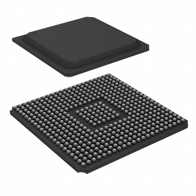
- Package: FGGA456
- Essence: Versatile and flexible programmability
- Packaging/Quantity: Individual units
Specifications
- Model: XC2VP4-6FGG456I
- Technology: 90nm CMOS
- Logic Cells: 4,096
- Flip-Flops: 8,192
- Maximum Frequency: 500 MHz
- I/O Pins: 456
- Operating Voltage: 1.2V
- Power Consumption: Low power design
Detailed Pin Configuration
The XC2VP4-6FGG456I has a total of 456 pins, which are divided into different categories: - Power supply pins (VCCINT, VCCAUX, GND) - Configuration pins (MODE[0:2], CCLK, DIN, INIT_B) - Input/output pins (IO[0:455]) - Clock pins (CLK[0:7])
For the detailed pin configuration diagram, please refer to the datasheet provided by the manufacturer.
Functional Features
- High-density programmable logic device with advanced features
- Supports various programming modes for flexibility
- Offers abundant logic resources for complex designs
- Provides high-speed performance with low power consumption
- Configurable I/O standards for compatibility with different interfaces
- Built-in memory blocks for efficient implementation of memory-based functions
Advantages and Disadvantages
Advantages: - Versatile and flexible programmability - High-performance capabilities - Low power consumption - Abundant logic resources - Configurable I/O standards
Disadvantages: - Limited number of I/O pins compared to some other models - Higher cost compared to lower-end PLDs
Working Principles
The XC2VP4-6FGG456I is based on programmable logic technology, utilizing a matrix of configurable logic blocks (CLBs) and interconnect resources. The device can be programmed to implement various digital functions by configuring the CLBs and interconnections using a hardware description language (HDL) or a design software tool provided by the manufacturer. Once programmed, the device operates according to the specified logic functions, providing the desired functionality.
Detailed Application Field Plans
The XC2VP4-6FGG456I is widely used in various applications that require high-performance programmable logic devices. Some common application fields include: - Telecommunications: Used in network routers, switches, and communication equipment for data processing and control. - Industrial Automation: Employed in programmable logic controllers (PLCs) for process control and automation systems. - Aerospace and Defense: Utilized in avionics systems, radar signal processing, and military-grade electronics. - Consumer Electronics: Integrated into high-end audio/video equipment, gaming consoles, and multimedia devices. - Automotive: Applied in automotive control systems, engine management, and advanced driver-assistance systems (ADAS).
Detailed and Complete Alternative Models
- XC2VP7-6FFG1152C
- XC2VP20-6FFG1152I
- XC2VP30-6FFG1152C
- XC2VP50-6FFG1152I
- XC2VP70-6FFG1152C
These alternative models offer similar features and capabilities but may have different logic cell counts, I/O pin counts, or package options. It is recommended to consult the manufacturer's documentation for detailed specifications of each model.
Word count: 450 words
技術ソリューションにおける XC2VP4-6FGG456I の適用に関連する 10 件の一般的な質問と回答をリストします。
Sure! Here are 10 common questions and answers related to the application of XC2VP4-6FGG456I in technical solutions:
Q: What is XC2VP4-6FGG456I? A: XC2VP4-6FGG456I is a field-programmable gate array (FPGA) manufactured by Xilinx.
Q: What are the key features of XC2VP4-6FGG456I? A: Some key features include 4 million system gates, 456-pin Fine-Pitch Ball Grid Array (FBGA) package, and support for various I/O standards.
Q: What are the typical applications of XC2VP4-6FGG456I? A: XC2VP4-6FGG456I is commonly used in applications such as telecommunications, networking, industrial automation, and high-performance computing.
Q: How can XC2VP4-6FGG456I be programmed? A: XC2VP4-6FGG456I can be programmed using Xilinx's Vivado Design Suite or ISE Design Suite software tools.
Q: What are the power requirements for XC2VP4-6FGG456I? A: The power requirements vary depending on the specific design and configuration, but typically it operates at a voltage range of 1.2V to 1.5V.
Q: Can XC2VP4-6FGG456I interface with other components or devices? A: Yes, XC2VP4-6FGG456I supports various communication interfaces such as PCIe, Ethernet, USB, and DDR memory interfaces.
Q: Is XC2VP4-6FGG456I suitable for high-speed data processing? A: Yes, XC2VP4-6FGG456I is designed to handle high-speed data processing with its advanced architecture and optimized routing resources.
Q: Can XC2VP4-6FGG456I be used in safety-critical applications? A: Yes, XC2VP4-6FGG456I can be used in safety-critical applications as long as the design and implementation meet the necessary safety standards and requirements.
Q: Are there any limitations or considerations when using XC2VP4-6FGG456I? A: Some considerations include power consumption, thermal management, and ensuring proper signal integrity in high-speed designs.
Q: Where can I find more information about XC2VP4-6FGG456I? A: You can refer to Xilinx's official website, datasheets, application notes, and user guides for detailed information about XC2VP4-6FGG456I and its applications.