

XC2S150-6PQG208C
Product Overview
Category
XC2S150-6PQG208C belongs to the category of Field Programmable Gate Arrays (FPGAs).
Use
This product is primarily used in digital logic circuits for various applications such as telecommunications, automotive, aerospace, and consumer electronics.
Characteristics
- High-performance programmable logic device
- Offers flexibility and reconfigurability
- Provides high-speed data processing capabilities
- Supports complex algorithms and designs
- Low power consumption
- Reliable and durable
Package
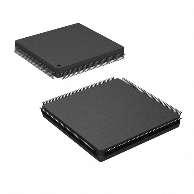
XC2S150-6PQG208C comes in a PQG208 package.
Essence
The essence of XC2S150-6PQG208C lies in its ability to provide a customizable and adaptable solution for implementing complex digital systems.
Packaging/Quantity
This product is typically packaged individually and is available in varying quantities depending on the manufacturer's specifications.
Specifications
- Model: XC2S150-6PQG208C
- Logic Cells: 150,000
- Speed Grade: 6
- Package Type: PQG208
- Operating Temperature Range: -40°C to 100°C
- Supply Voltage: 1.2V
- I/O Standards: LVCMOS, LVTTL, HSTL, SSTL, LVDS, RSDS
Detailed Pin Configuration
The XC2S150-6PQG208C FPGA has a total of 208 pins. The pin configuration varies based on the specific requirements of the application and can be found in the product datasheet provided by the manufacturer.
Functional Features
- Configurable logic blocks for implementing custom logic functions
- Dedicated memory blocks for storing data
- Built-in arithmetic functions for mathematical operations
- Programmable interconnects for connecting different components
- Clock management resources for precise timing control
- On-chip configuration memory for storing the design
Advantages and Disadvantages
Advantages
- Flexibility: Allows for easy modification and reconfiguration of digital circuits.
- Time-to-Market: Reduces development time by eliminating the need for custom hardware.
- Cost-Effective: Eliminates the need for multiple discrete components, reducing overall system cost.
- High Performance: Provides fast data processing capabilities suitable for demanding applications.
Disadvantages
- Complexity: Designing and programming FPGAs can be challenging and requires specialized knowledge.
- Power Consumption: FPGAs tend to consume more power compared to application-specific integrated circuits (ASICs).
- Limited Resources: The available logic cells and memory blocks may not be sufficient for extremely complex designs.
Working Principles
XC2S150-6PQG208C operates based on the principles of configurable logic. It consists of a matrix of programmable logic cells interconnected through programmable routing resources. These logic cells can be configured to implement various digital functions, allowing designers to create custom logic circuits.
The FPGA is programmed using a Hardware Description Language (HDL) such as VHDL or Verilog. The HDL code describes the desired functionality of the circuit, which is then synthesized and mapped onto the FPGA. Once programmed, the FPGA can execute the desired logic operations.
Detailed Application Field Plans
XC2S150-6PQG208C finds applications in a wide range of fields, including:
- Telecommunications: Used in network routers, switches, and base stations for high-speed data processing and protocol handling.
- Automotive: Employed in automotive electronics for engine control units, advanced driver-assistance systems (ADAS), and infotainment systems.
- Aerospace: Utilized in avionics systems for flight control, communication, and navigation.
- Consumer Electronics: Integrated into devices such as smartphones, tablets, and gaming consoles for accelerated graphics processing and multimedia functions.
Detailed and Complete Alternative Models
- XC2S50-6PQG208C: A lower-capacity version of the XC2S150-6PQG208C with 50,000 logic cells.
- XC2S200-6PQG208C: A higher-capacity version of the XC2S150-6PQG208C with 200,000 logic cells.
- XC2S300-6PQG208C: An even higher-capacity version of the XC2S150-6PQG208C with 300,000 logic cells.
These alternative models provide options with varying logic cell capacities to suit different application requirements.
In conclusion, XC2S150-6PQG208C is a high-performance FPGA that offers flexibility, reconfigurability, and high-speed data processing capabilities. It finds applications in various fields and provides advantages such as cost-effectiveness and time-to-market benefits. However, it also has disadvantages related to complexity and
技術ソリューションにおける XC2S150-6PQG208C の適用に関連する 10 件の一般的な質問と回答をリストします。
Sure! Here are 10 common questions and answers related to the application of XC2S150-6PQG208C in technical solutions:
Question: What is XC2S150-6PQG208C?
Answer: XC2S150-6PQG208C is a specific model of Xilinx Spartan-II FPGA (Field-Programmable Gate Array) with 150,000 system gates.Question: What are the key features of XC2S150-6PQG208C?
Answer: Some key features of XC2S150-6PQG208C include 150,000 system gates, 6ns maximum pin-to-pin delay, and 208-pin Quad Flat Pack (QFP) package.Question: What are the typical applications of XC2S150-6PQG208C?
Answer: XC2S150-6PQG208C is commonly used in various technical solutions such as digital signal processing, embedded systems, telecommunications, and industrial automation.Question: How can XC2S150-6PQG208C be programmed?
Answer: XC2S150-6PQG208C can be programmed using Xilinx's programming tools like Vivado or ISE Design Suite, which allow users to design and implement their own logic circuits.Question: What is the power supply requirement for XC2S150-6PQG208C?
Answer: XC2S150-6PQG208C requires a power supply voltage of 3.3V.Question: Can XC2S150-6PQG208C be used in high-speed applications?
Answer: Yes, XC2S150-6PQG208C has a maximum pin-to-pin delay of 6ns, making it suitable for high-speed applications.Question: Does XC2S150-6PQG208C support external memory interfaces?
Answer: Yes, XC2S150-6PQG208C supports various external memory interfaces like SDRAM, DDR, and Flash memory.Question: Can XC2S150-6PQG208C be used in low-power applications?
Answer: Yes, XC2S150-6PQG208C has power-saving features like clock gating and power management modes, making it suitable for low-power applications.Question: Is XC2S150-6PQG208C compatible with other Xilinx FPGAs?
Answer: Yes, XC2S150-6PQG208C is part of the Spartan-II FPGA family and is compatible with other members of the same family.Question: Where can I find more information about XC2S150-6PQG208C?
Answer: You can find more detailed information about XC2S150-6PQG208C in the official documentation provided by Xilinx, including datasheets and user guides.