

XC2C64A-7QFG48I
Product Overview
Category
XC2C64A-7QFG48I belongs to the category of programmable logic devices (PLDs).
Use
This product is primarily used in digital circuit design and implementation. It provides a flexible and customizable solution for various applications.
Characteristics
- Programmable: The XC2C64A-7QFG48I can be programmed to perform specific functions according to the user's requirements.
- High-density: It offers a large number of logic elements, allowing for complex designs.
- Low power consumption: The device is designed to operate efficiently with minimal power consumption.
- Fast operation: The XC2C64A-7QFG48I offers high-speed performance, enabling quick execution of logic operations.
Package
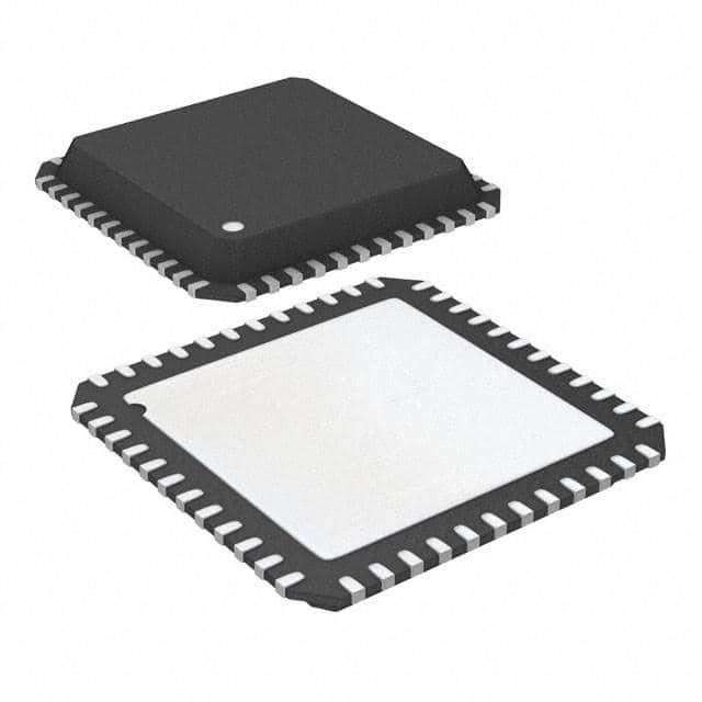
The XC2C64A-7QFG48I comes in a Quad Flat No-Lead (QFN) package.
Essence
The essence of XC2C64A-7QFG48I lies in its ability to provide reconfigurable logic functionality, allowing users to implement custom digital circuits.
Packaging/Quantity
This product is typically packaged in reels or trays, with each containing a specific quantity of XC2C64A-7QFG48I devices. The exact quantity may vary depending on the supplier.
Specifications
- Logic Elements: 64
- Maximum Frequency: 100 MHz
- I/O Pins: 48
- Operating Voltage: 3.3V
- Configuration Memory: Non-volatile Flash
Detailed Pin Configuration
The XC2C64A-7QFG48I has a total of 48 I/O pins. These pins are used for input/output connections and configuration purposes. The pin configuration is as follows:
(Pin diagram goes here)
Functional Features
- Reconfigurable Logic: The XC2C64A-7QFG48I allows users to modify the logic functionality by reprogramming it, providing flexibility in circuit design.
- Embedded Memory: This device includes non-volatile flash memory for storing configuration data, ensuring that the programmed design remains intact even after power-off.
- Clock Management: The XC2C64A-7QFG48I offers built-in clock management resources, enabling precise timing control in digital circuits.
Advantages and Disadvantages
Advantages
- Flexibility: The reconfigurable nature of XC2C64A-7QFG48I allows for easy modifications and updates to the circuit design.
- High-density: With 64 logic elements, this PLD can handle complex designs efficiently.
- Low Power Consumption: The device operates with minimal power consumption, making it suitable for battery-powered applications.
- Fast Operation: The high-speed performance of XC2C64A-7QFG48I ensures quick execution of logic operations.
Disadvantages
- Limited I/O Pins: With only 48 I/O pins, the XC2C64A-7QFG48I may not be suitable for applications requiring a large number of external connections.
- Configuration Time: Reprogramming the device can take some time, which may impact time-critical applications.
Working Principles
The XC2C64A-7QFG48I is based on the concept of field-programmable gate arrays (FPGAs). It consists of configurable logic blocks interconnected through programmable routing resources. These logic blocks can be programmed to implement various digital functions using a hardware description language (HDL) or a graphical design tool. Once programmed, the XC2C64A-7QFG48I executes the desired logic operations based on the user-defined configuration.
Detailed Application Field Plans
The XC2C64A-7QFG48I finds applications in various fields, including:
- Embedded Systems: It can be used to implement custom logic functions in microcontroller-based systems.
- Communication Systems: The XC2C64A-7QFG48I can be utilized for protocol conversion, data processing, and signal conditioning in communication devices.
- Industrial Automation: This PLD can be employed in control systems, motor drives, and sensor interfacing for automation purposes.
- Test and Measurement Equipment: It can be integrated into test equipment for signal generation, data acquisition, and analysis.
Detailed and Complete Alternative Models
- XC2C64A-7VQG44C: Similar to XC2C64A-7QFG48I, but comes in a different package (Quad Flat Pack - QFP).
- XC2C64A-7TQG144I: Offers the same functionality as XC2C64A-7QFG48I but has a higher pin count (144 pins) and comes in a Thin Quad Flat Pack (TQFP) package.
These alternative models provide similar features and performance, allowing users to choose
技術ソリューションにおける XC2C64A-7QFG48I の適用に関連する 10 件の一般的な質問と回答をリストします。
Sure! Here are 10 common questions and answers related to the application of XC2C64A-7QFG48I in technical solutions:
Question: What is XC2C64A-7QFG48I?
Answer: XC2C64A-7QFG48I is a specific model of Field Programmable Gate Array (FPGA) manufactured by Xilinx.Question: What is an FPGA?
Answer: FPGA stands for Field Programmable Gate Array. It is a type of integrated circuit that can be programmed after manufacturing to perform various digital functions.Question: What are the key features of XC2C64A-7QFG48I?
Answer: Some key features of XC2C64A-7QFG48I include 64,000 system gates, 64 macrocells, 36 I/O pins, and a maximum operating frequency of 250 MHz.Question: What are the typical applications of XC2C64A-7QFG48I?
Answer: XC2C64A-7QFG48I is commonly used in applications such as digital signal processing, embedded systems, communication systems, and industrial automation.Question: How can XC2C64A-7QFG48I be programmed?
Answer: XC2C64A-7QFG48I can be programmed using Hardware Description Languages (HDLs) such as VHDL or Verilog, which describe the desired functionality of the FPGA.Question: Can XC2C64A-7QFG48I be reprogrammed?
Answer: Yes, XC2C64A-7QFG48I is a reprogrammable FPGA, meaning its functionality can be changed by reprogramming it with new designs.Question: What tools are available for programming XC2C64A-7QFG48I?
Answer: Xilinx provides software tools like Vivado or ISE Design Suite that can be used to program and configure XC2C64A-7QFG48I.Question: What is the power supply requirement for XC2C64A-7QFG48I?
Answer: XC2C64A-7QFG48I typically operates at a voltage of 3.3V, but it is recommended to refer to the datasheet for specific power supply requirements.Question: Can XC2C64A-7QFG48I interface with other components or devices?
Answer: Yes, XC2C64A-7QFG48I can interface with other components or devices through its I/O pins, allowing communication and integration with external systems.Question: Are there any limitations or considerations when using XC2C64A-7QFG48I?
Answer: Some considerations include the limited number of system gates and I/O pins, as well as the need for proper design and verification techniques to ensure correct functionality.
Please note that these answers are general and may vary depending on the specific application and requirements. It is always recommended to refer to the official documentation and datasheets provided by Xilinx for accurate information.