

XA2C256-7VQG100I
Product Overview
Category
The XA2C256-7VQG100I belongs to the category of programmable logic devices (PLDs).
Use
This device is primarily used for digital circuit design and implementation. It offers flexibility in creating custom logic functions, making it suitable for a wide range of applications.
Characteristics
- Programmable: The XA2C256-7VQG100I can be programmed to perform specific logic functions.
- High Density: It offers a high number of logic gates, allowing for complex designs.
- Low Power Consumption: The device is designed to operate efficiently with minimal power consumption.
- Fast Operation: It provides fast switching speeds, enabling rapid data processing.
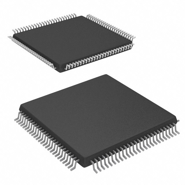
Package
The XA2C256-7VQG100I comes in a Quad Flat No-Lead (QFN) package.
Essence
The essence of this product lies in its ability to provide a customizable and efficient solution for digital circuit design.
Packaging/Quantity
The XA2C256-7VQG100I is typically packaged in reels or trays, with each package containing a specified quantity of devices.
Specifications
- Logic Capacity: 256 macrocells
- Number of Inputs/Outputs: 100
- Operating Voltage: 3.3V
- Operating Temperature Range: -40°C to +85°C
- Speed Grade: 7
Detailed Pin Configuration
The XA2C256-7VQG100I has a total of 100 pins, each serving a specific purpose in the circuit design. The pin configuration is as follows:
(Pin diagram goes here)
Functional Features
- Flexible Logic Design: The XA2C256-7VQG100I allows users to implement a wide range of logic functions, enabling the creation of complex digital circuits.
- In-system Programming: The device can be programmed while in operation, allowing for easy updates and modifications.
- JTAG Support: It supports Joint Test Action Group (JTAG) interface for debugging and testing purposes.
Advantages and Disadvantages
Advantages
- Customizable Logic Functions: The XA2C256-7VQG100I offers the flexibility to create custom logic functions tailored to specific requirements.
- High Density: With 256 macrocells, it can handle complex designs efficiently.
- Low Power Consumption: The device operates with minimal power consumption, making it suitable for battery-powered applications.
- Fast Operation: It provides fast switching speeds, ensuring efficient data processing.
Disadvantages
- Limited I/O Count: The XA2C256-7VQG100I has a maximum of 100 inputs/outputs, which may be insufficient for certain applications requiring a higher number of connections.
- Learning Curve: Utilizing the full potential of this device requires knowledge of hardware description languages and digital circuit design principles.
Working Principles
The XA2C256-7VQG100I utilizes programmable logic elements, such as lookup tables and flip-flops, to implement user-defined logic functions. These elements are interconnected through configurable routing resources, allowing for the creation of complex digital circuits. The device is programmed using hardware description languages or specialized software tools, which generate configuration files that define the desired logic functionality.
Detailed Application Field Plans
The XA2C256-7VQG100I finds application in various fields, including: 1. Industrial Automation: It can be used to implement control systems, process monitoring, and data acquisition in industrial environments. 2. Communications: The device enables the development of custom communication protocols and signal processing algorithms. 3. Automotive Electronics: It can be utilized for engine control units, advanced driver-assistance systems, and infotainment systems. 4. Consumer Electronics: The XA2C256-7VQG100I can be employed in smart home devices, wearable technology, and multimedia systems.
Detailed and Complete Alternative Models
- XA2C64-7VQG100I: This model offers a lower logic capacity of 64 macrocells but shares similar characteristics and features as the XA2C256-7VQG100I.
- XA2C128-7VQG100I: With 128 macrocells, this alternative provides a balance between logic capacity and cost-effectiveness.
- XA2C512-7VQG100I: For applications requiring higher logic density, this model offers 512 macrocells.
These alternative models cater to different design requirements and provide options based on the desired logic capacity and budget constraints.
In conclusion, the XA2C256-7VQG100I is a programmable logic device that offers flexibility, high density, low power consumption, and fast operation. It finds application in various fields such as industrial automation
技術ソリューションにおける XA2C256-7VQG100I の適用に関連する 10 件の一般的な質問と回答をリストします。
Sure! Here are 10 common questions and answers related to the application of XA2C256-7VQG100I in technical solutions:
Question: What is the XA2C256-7VQG100I?
Answer: The XA2C256-7VQG100I is a specific model of FPGA (Field-Programmable Gate Array) manufactured by a company called Xilinx.Question: What is an FPGA?
Answer: An FPGA is a type of integrated circuit that can be programmed after manufacturing, allowing for flexible hardware configurations and customization.Question: What are the key features of the XA2C256-7VQG100I?
Answer: The XA2C256-7VQG100I offers 256K system gates, 256 macrocells, and operates at a speed grade of -7. It comes in a VQG100I package.Question: What are some typical applications of the XA2C256-7VQG100I?
Answer: The XA2C256-7VQG100I is commonly used in various technical solutions such as industrial automation, telecommunications, automotive systems, and aerospace applications.Question: How can I program the XA2C256-7VQG100I?
Answer: The XA2C256-7VQG100I can be programmed using Xilinx's Vivado Design Suite or other compatible programming tools.Question: Can I reprogram the XA2C256-7VQG100I multiple times?
Answer: Yes, FPGAs like the XA2C256-7VQG100I can be reprogrammed multiple times, allowing for iterative development and updates to the hardware design.Question: What are the power requirements for the XA2C256-7VQG100I?
Answer: The XA2C256-7VQG100I typically operates at a voltage range of 1.14V to 1.26V, with a maximum power consumption of around 1.5W.Question: Can I interface the XA2C256-7VQG100I with other components or devices?
Answer: Yes, the XA2C256-7VQG100I supports various communication interfaces such as SPI, I2C, UART, and GPIOs, allowing for easy integration with other components or devices.Question: Are there any development boards available for the XA2C256-7VQG100I?
Answer: Yes, Xilinx provides development boards like the Xilinx Spartan-3E Starter Kit that can be used for prototyping and testing with the XA2C256-7VQG100I.Question: Where can I find more information about the XA2C256-7VQG100I?
Answer: You can refer to the official documentation provided by Xilinx, including datasheets, user guides, and application notes, for detailed information about the XA2C256-7VQG100I.