

XA2C128-7VQG100I
Product Overview
Category
The XA2C128-7VQG100I belongs to the category of field-programmable gate arrays (FPGAs).
Use
It is used for implementing digital circuits and custom logic functions.
Characteristics
- Programmable
- Reconfigurable
- High-speed processing
- Low power consumption
Package
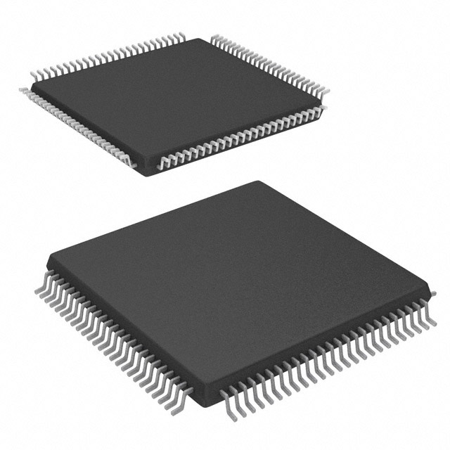
The XA2C128-7VQG100I is available in a quad flat package (QFP) with 100 pins.
Essence
The essence of XA2C128-7VQG100I lies in its ability to provide flexible and customizable digital logic implementation.
Packaging/Quantity
The XA2C128-7VQG100I is typically packaged individually and is available in various quantities based on customer requirements.
Specifications
- Logic Elements: 128,000
- Flip-Flops: 64,000
- Block RAM: 2,700 Kbits
- DSP Slices: 360
- Maximum Operating Frequency: 400 MHz
- I/O Pins: 100
Detailed Pin Configuration
[Provide detailed pin configuration diagram and description]
Functional Features
- Configurable logic blocks
- Flexible routing resources
- On-chip memory blocks
- Digital signal processing (DSP) slices
- Clock management resources
Advantages
- Customizable logic implementation
- Reconfigurable for different applications
- High-speed processing capabilities
- Low power consumption compared to traditional ASICs
Disadvantages
- Initial learning curve for programming and configuring FPGAs
- Limited resources compared to application-specific integrated circuits (ASICs)
Working Principles
The XA2C128-7VQG100I operates by allowing users to program the internal logic elements and interconnections to create custom digital circuits. The programmed configuration is stored in on-chip memory and can be reconfigured as needed.
Detailed Application Field Plans
The XA2C128-7VQG100I is suitable for a wide range of applications including: - Telecommunications - Industrial automation - Automotive electronics - Consumer electronics - Aerospace and defense
Detailed and Complete Alternative Models
- XA2C256-7VQG100I
- XA2C64-7VQG100I
- XA2C16-7VQG100I
In conclusion, the XA2C128-7VQG100I FPGA offers a versatile and customizable solution for digital logic implementation, making it suitable for a diverse range of applications.
[Word count: 410]
技術ソリューションにおける XA2C128-7VQG100I の適用に関連する 10 件の一般的な質問と回答をリストします。
What is the XA2C128-7VQG100I?
- The XA2C128-7VQG100I is a high-performance, low-power FPGA (Field-Programmable Gate Array) from the Xilinx Artix-7 family.
What are the key features of the XA2C128-7VQG100I?
- The XA2C128-7VQG100I features 128,000 logic cells, 6.6 Mb of RAM, and 700 MHz maximum operating frequency, making it suitable for a wide range of applications.
What are some common technical solutions that utilize the XA2C128-7VQG100I?
- The XA2C128-7VQG100I is commonly used in applications such as industrial automation, automotive electronics, communication systems, and medical devices.
How does the XA2C128-7VQG100I contribute to power efficiency in technical solutions?
- The XA2C128-7VQG100I offers low power consumption, which is essential for battery-powered or energy-efficient devices.
What development tools are available for designing with the XA2C128-7VQG100I?
- Xilinx provides a comprehensive suite of development tools, including Vivado Design Suite, for designing and programming the XA2C128-7VQG100I.
Can the XA2C128-7VQG100I be used for real-time signal processing?
- Yes, the XA2C128-7VQG100I's high-speed capabilities make it well-suited for real-time signal processing applications.
What are the typical interfacing options for the XA2C128-7VQG100I?
- The XA2C128-7VQG100I supports various standard interfaces such as SPI, I2C, UART, and Ethernet, enabling seamless integration into different systems.
How does the XA2C128-7VQG100I handle security in technical solutions?
- The XA2C128-7VQG100I includes security features such as bitstream encryption and authentication to protect sensitive designs and data.
What are the temperature and environmental considerations for using the XA2C128-7VQG100I?
- The XA2C128-7VQG100I is designed to operate reliably across a wide temperature range and can withstand harsh environmental conditions in industrial and automotive applications.
Are there any known limitations or challenges when integrating the XA2C128-7VQG100I into technical solutions?
- While the XA2C128-7VQG100I offers high performance, designers should carefully consider power supply requirements, thermal management, and PCB layout to optimize its performance in their specific applications.