

SI3909DV-T1-GE3
Product Category
The SI3909DV-T1-GE3 belongs to the category of power MOSFETs, which are semiconductor devices used for switching and amplifying electronic signals in various applications.
Basic Information Overview
- Category: Power MOSFET
- Use: Switching and amplifying electronic signals
- Characteristics: High efficiency, low on-resistance, fast switching speed
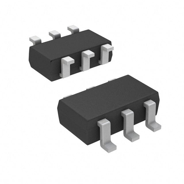
- Package: DFN (Dual Flat No-Lead)
- Essence: Efficient power management
- Packaging/Quantity: Tape & Reel, 3000 units per reel
Specifications
- Voltage Rating: 30V
- Current Rating: 8.3A
- On-Resistance: 10mΩ
- Package Type: DFN5x6
Detailed Pin Configuration
The SI3909DV-T1-GE3 features a DFN5x6 package with the following pin configuration: 1. Gate 2. Source 3. Drain 4. N/C (Not Connected) 5. Source
Functional Features
- Low on-resistance for minimal power loss
- Fast switching speed for efficient operation
- Enhanced thermal performance for reliability
Advantages and Disadvantages
Advantages: - High efficiency - Low power dissipation - Compact package size
Disadvantages: - Sensitive to overvoltage conditions - Limited maximum current handling capability
Working Principles
The SI3909DV-T1-GE3 operates based on the principle of field-effect transistors, where the voltage applied to the gate terminal controls the flow of current between the source and drain terminals. By modulating the gate voltage, the device can efficiently switch and amplify electronic signals.
Detailed Application Field Plans
The SI3909DV-T1-GE3 is ideally suited for use in various applications, including: - Power supplies - DC-DC converters - Motor control - LED lighting - Battery management systems
Detailed and Complete Alternative Models
SI2309DS-T1-GE3
- Voltage Rating: 20V
- Current Rating: 4.3A
- On-Resistance: 25mΩ
- Package Type: DFN5x6
SI4435DY-T1-GE3
- Voltage Rating: 30V
- Current Rating: 12A
- On-Resistance: 6mΩ
- Package Type: DFN5x6
In conclusion, the SI3909DV-T1-GE3 power MOSFET offers high efficiency, fast switching speed, and compact packaging, making it an ideal choice for various electronic applications requiring efficient power management.
Word count: 366
技術ソリューションにおける SI3909DV-T1-GE3 の適用に関連する 10 件の一般的な質問と回答をリストします。
What is the maximum voltage rating of SI3909DV-T1-GE3?
- The maximum voltage rating of SI3909DV-T1-GE3 is 30V.
What is the typical on-resistance of SI3909DV-T1-GE3?
- The typical on-resistance of SI3909DV-T1-GE3 is 0.022 ohms.
What is the maximum continuous drain current of SI3909DV-T1-GE3?
- The maximum continuous drain current of SI3909DV-T1-GE3 is 7.3A.
What is the gate threshold voltage of SI3909DV-T1-GE3?
- The gate threshold voltage of SI3909DV-T1-GE3 is typically 1.5V.
What are the typical applications for SI3909DV-T1-GE3?
- SI3909DV-T1-GE3 is commonly used in load switch, power management, and battery protection applications.
What is the package type of SI3909DV-T1-GE3?
- SI3909DV-T1-GE3 comes in a compact and efficient PowerPAK® SC-70 package.
What is the operating temperature range of SI3909DV-T1-GE3?
- The operating temperature range of SI3909DV-T1-GE3 is -55°C to 150°C.
Does SI3909DV-T1-GE3 have built-in ESD protection?
- Yes, SI3909DV-T1-GE3 features built-in ESD protection, enhancing its robustness in various applications.
Is SI3909DV-T1-GE3 suitable for automotive applications?
- Yes, SI3909DV-T1-GE3 is AEC-Q101 qualified, making it suitable for automotive applications.
What are the key advantages of using SI3909DV-T1-GE3 in technical solutions?
- Some key advantages of SI3909DV-T1-GE3 include low on-resistance, high current capability, small package size, and reliable performance in demanding environments.