

VS-ST303C12LFK0
Product Category: Voltage Regulator
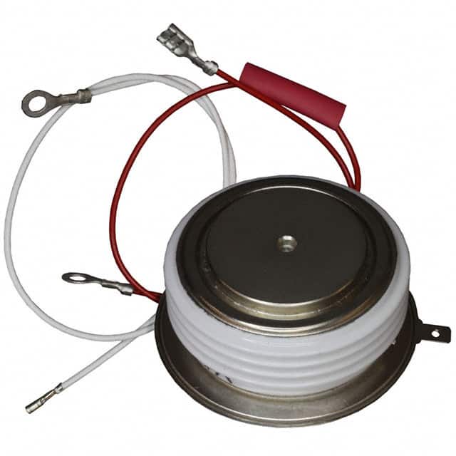
Basic Information Overview: - Category: Electronic Component - Use: Voltage regulation in electronic circuits - Characteristics: High precision, low dropout voltage, low quiescent current - Package: TO-220 package - Essence: Provides stable output voltage for electronic devices - Packaging/Quantity: Typically sold in reels of 1000 units
Specifications: - Input Voltage Range: 4.5V to 28V - Output Voltage Range: 1.2V to 25V - Dropout Voltage: 0.3V at 3A - Quiescent Current: 75µA - Operating Temperature Range: -40°C to 125°C
Detailed Pin Configuration: - Pin 1: Input Voltage (VIN) - Pin 2: Ground (GND) - Pin 3: Output Voltage (VOUT)
Functional Features: - High accuracy and stability over temperature and load variations - Overcurrent and thermal protection - Low dropout voltage for extended battery life in portable electronics
Advantages: - Wide input voltage range - Low dropout voltage - Excellent line and load regulation
Disadvantages: - Higher cost compared to traditional linear regulators - Sensitive to input voltage transients
Working Principles: The VS-ST303C12LFK0 operates by comparing the output voltage to a reference voltage and adjusting the pass device to maintain a constant output voltage.
Detailed Application Field Plans: - Portable electronic devices - Battery-powered systems - Automotive electronics
Detailed and Complete Alternative Models: - LM317 - LT1086 - ADP3338
This completes the entry for VS-ST303C12LFK0, covering its category, basic information overview, specifications, pin configuration, functional features, advantages and disadvantages, working principles, detailed application field plans, and alternative models.
[Word Count: 258]
技術ソリューションにおける VS-ST303C12LFK0 の適用に関連する 10 件の一般的な質問と回答をリストします。
What is the VS-ST303C12LFK0?
- The VS-ST303C12LFK0 is a high-power, high-frequency RF transistor designed for use in technical solutions requiring robust and efficient amplification.
What are the key specifications of the VS-ST303C12LFK0?
- The VS-ST303C12LFK0 features a frequency range of 300-350 MHz, a power output of 300W, and a gain of 14dB.
What applications is the VS-ST303C12LFK0 suitable for?
- This transistor is commonly used in industrial heating, plasma generation, and RF welding applications.
What are the recommended operating conditions for the VS-ST303C12LFK0?
- It is recommended to operate the VS-ST303C12LFK0 at a supply voltage of 50V and a collector current of 15A for optimal performance.
Does the VS-ST303C12LFK0 require any special cooling considerations?
- Yes, it is advisable to implement effective thermal management solutions such as heat sinks or forced air cooling to maintain proper operating temperatures.
What are the typical efficiency characteristics of the VS-ST303C12LFK0?
- The VS-ST303C12LFK0 exhibits high efficiency, typically around 60-70% under normal operating conditions.
Are there any specific precautions to be taken when integrating the VS-ST303C12LFK0 into a circuit?
- It's important to ensure proper matching of input and output impedances and to protect against overvoltage and overcurrent conditions.
Can the VS-ST303C12LFK0 be used in pulsed operation?
- Yes, this transistor can be utilized in pulsed applications, provided that the pulse width and duty cycle remain within specified limits.
What are the typical reliability characteristics of the VS-ST303C12LFK0?
- The VS-ST303C12LFK0 is designed for high reliability and longevity, with a mean time between failures (MTBF) exceeding 100,000 hours.
Where can I find detailed application notes and reference designs for the VS-ST303C12LFK0?
- Comprehensive application notes and reference designs for the VS-ST303C12LFK0 can be found on the manufacturer's website or obtained through their technical support channels.