

TC74ACT374P
Product Overview
Category
The TC74ACT374P belongs to the category of integrated circuits (ICs).
Use
This IC is commonly used in digital electronics for data storage and transfer applications.
Characteristics
- High-speed operation
- Low power consumption
- Wide operating voltage range
- Schmitt trigger inputs for noise immunity
- 3-state outputs for bus-oriented applications
Package
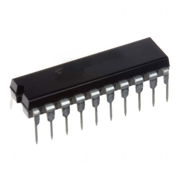
The TC74ACT374P is available in a 20-pin plastic dual in-line package (PDIP).
Essence
The essence of TC74ACT374P lies in its ability to store and transfer digital data efficiently and reliably.
Packaging/Quantity
The IC is typically packaged in reels or tubes, with a quantity of 250 units per reel/tube.
Specifications
- Supply Voltage: 2.0V to 6.0V
- Input Voltage: 0V to VCC
- Output Voltage: 0V to VCC
- Operating Temperature Range: -40°C to +85°C
- Maximum Clock Frequency: 100MHz
Detailed Pin Configuration
The TC74ACT374P has a total of 20 pins, each serving a specific function. The pin configuration is as follows:
- D0: Data input 0
- D1: Data input 1
- D2: Data input 2
- D3: Data input 3
- D4: Data input 4
- D5: Data input 5
- D6: Data input 6
- D7: Data input 7
- GND: Ground
- Q0: Output 0
- Q1: Output 1
- Q2: Output 2
- Q3: Output 3
- Q4: Output 4
- Q5: Output 5
- Q6: Output 6
- Q7: Output 7
- CP: Clock input
- OE: Output enable
- VCC: Power supply
Functional Features
The TC74ACT374P offers the following functional features:
- Data Storage: The IC can store data on its inputs and retain it until a clock signal is received.
- Data Transfer: Upon receiving a clock signal, the stored data is transferred to the corresponding output pins.
- 3-State Outputs: The outputs can be put in a high-impedance state, allowing multiple devices to share a common bus.
Advantages and Disadvantages
Advantages
- High-speed operation enables efficient data transfer.
- Low power consumption makes it suitable for battery-powered applications.
- Wide operating voltage range allows compatibility with various systems.
- Schmitt trigger inputs provide noise immunity, ensuring reliable operation.
- 3-state outputs facilitate bus-oriented applications.
Disadvantages
- Limited number of data inputs and outputs (8 bits).
- Not suitable for applications requiring larger data storage capacities.
Working Principles
The TC74ACT374P operates based on the principles of flip-flops and latches. When a clock signal is applied, the current state of the data inputs is captured and stored. This stored data is then transferred to the outputs upon the next clock cycle. The 3-state outputs allow the IC to disconnect from the bus when not actively driving it.
Detailed Application Field Plans
The TC74ACT374P finds applications in various fields, including:
- Microcontrollers: Used for interfacing with external memory or peripherals.
- Communication Systems: Facilitates data buffering and transfer between different components.
- Industrial Automation: Enables control and monitoring of digital signals in automated systems.
- Automotive Electronics: Used in vehicle control units for data storage and transfer.
Detailed and Complete Alternative Models
- SN74ACT374: Similar functionality, available in different package options.
- CD74ACT374: Comparable performance, suitable for high-speed applications.
- MC74ACT374: Alternative manufacturer, offers similar features and specifications.
These alternative models can be considered based on specific requirements and availability.
Word count: 523 words
技術ソリューションにおける TC74ACT374P の適用に関連する 10 件の一般的な質問と回答をリストします。
Sure! Here are 10 common questions and answers related to the application of TC74ACT374P in technical solutions:
Q: What is TC74ACT374P? A: TC74ACT374P is a type of octal D-type flip-flop integrated circuit (IC) that can be used for various digital logic applications.
Q: What is the operating voltage range of TC74ACT374P? A: The operating voltage range of TC74ACT374P is typically between 4.5V and 5.5V.
Q: How many flip-flops are there in TC74ACT374P? A: TC74ACT374P consists of 8 individual D-type flip-flops, making it an octal flip-flop IC.
Q: What is the maximum clock frequency supported by TC74ACT374P? A: TC74ACT374P can support clock frequencies up to 100 MHz.
Q: Can TC74ACT374P be used for both synchronous and asynchronous operations? A: Yes, TC74ACT374P can be used for both synchronous and asynchronous operations depending on the application requirements.
Q: What is the output drive capability of TC74ACT374P? A: TC74ACT374P has a typical output drive capability of ±24 mA, which makes it suitable for driving various loads.
Q: Does TC74ACT374P have any built-in protection features? A: Yes, TC74ACT374P includes built-in ESD protection diodes to safeguard against electrostatic discharge events.
Q: Can TC74ACT374P operate in a wide temperature range? A: Yes, TC74ACT374P is designed to operate in a wide temperature range, typically between -40°C and 85°C.
Q: What is the package type of TC74ACT374P? A: TC74ACT374P is available in a standard 20-pin plastic DIP (Dual In-line Package) or SOIC (Small Outline Integrated Circuit) package.
Q: What are some typical applications of TC74ACT374P? A: TC74ACT374P can be used in various applications such as data storage, address latching, register buffering, and general-purpose digital logic circuits.
Please note that these answers are general and may vary depending on the specific datasheet and manufacturer's specifications for TC74ACT374P.