

XC6120C272NR-G
Product Overview
Category
XC6120C272NR-G belongs to the category of integrated circuits (ICs).
Use
This product is commonly used in electronic devices for voltage regulation and power management.
Characteristics
- Voltage regulation capabilities
- Power management features
- Compact size
- High efficiency
- Low power consumption
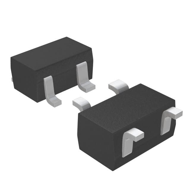
Package
XC6120C272NR-G is available in a small form factor package, making it suitable for space-constrained applications.
Essence
The essence of XC6120C272NR-G lies in its ability to regulate voltage and manage power efficiently, ensuring stable operation of electronic devices.
Packaging/Quantity
This product is typically packaged in reels or tubes, with a quantity of 3000 units per reel/tube.
Specifications
- Input Voltage Range: 2.5V - 6.0V
- Output Voltage Range: 1.2V - 5.5V
- Maximum Output Current: 200mA
- Dropout Voltage: 100mV @ 100mA
- Quiescent Current: 30µA (typical)
- Operating Temperature Range: -40°C to +85°C
Detailed Pin Configuration
XC6120C272NR-G has the following pin configuration:
- VIN: Input voltage pin
- GND: Ground pin
- EN: Enable pin
- VOUT: Output voltage pin
Functional Features
- Voltage regulation: XC6120C272NR-G ensures a stable output voltage within the specified range.
- Power management: This IC efficiently manages power consumption, reducing energy waste.
- Enable pin: The EN pin allows for easy control of the device's operation.
Advantages and Disadvantages
Advantages
- Compact size enables usage in space-constrained applications.
- High efficiency results in reduced power consumption.
- Wide input and output voltage ranges provide flexibility in various applications.
Disadvantages
- Limited maximum output current may not be suitable for high-power devices.
- Dropout voltage of 100mV may affect performance in low-voltage applications.
Working Principles
XC6120C272NR-G utilizes a combination of internal circuitry and feedback mechanisms to regulate the output voltage. It continuously monitors the input voltage and adjusts its internal components to maintain a stable output voltage, even under varying load conditions.
Detailed Application Field Plans
XC6120C272NR-G finds applications in various electronic devices, including but not limited to: - Mobile phones - Portable media players - Digital cameras - Wearable devices - IoT devices
In these applications, XC6120C272NR-G ensures reliable voltage regulation and efficient power management, contributing to the overall performance and longevity of the devices.
Detailed and Complete Alternative Models
Some alternative models that offer similar functionality to XC6120C272NR-G are: - XC6206P332MR-G - XC6220B332MR-G - XC6219B332MR-G - XC6220C332MR-G
These models share comparable specifications and features, providing users with options based on their specific requirements.
Word count: 411
技術ソリューションにおける XC6120C272NR-G の適用に関連する 10 件の一般的な質問と回答をリストします。
Sure! Here are 10 common questions and answers related to the application of XC6120C272NR-G in technical solutions:
Q: What is XC6120C272NR-G? A: XC6120C272NR-G is a voltage detector IC (integrated circuit) manufactured by Torex Semiconductor. It is commonly used for monitoring power supply voltages in various electronic devices.
Q: What is the operating voltage range of XC6120C272NR-G? A: The operating voltage range of XC6120C272NR-G is typically between 0.8V and 6.0V.
Q: How does XC6120C272NR-G work? A: XC6120C272NR-G works by comparing the input voltage with a fixed reference voltage. When the input voltage falls below or exceeds the specified threshold, it triggers an output signal.
Q: What is the output type of XC6120C272NR-G? A: XC6120C272NR-G has an open-drain output type, which means it can sink current but cannot source current.
Q: What is the typical quiescent current consumption of XC6120C272NR-G? A: The typical quiescent current consumption of XC6120C272NR-G is very low, usually around 1.0µA.
Q: Can XC6120C272NR-G be used for overvoltage protection? A: No, XC6120C272NR-G is primarily designed for undervoltage detection. It does not provide overvoltage protection functionality.
Q: What is the typical reset delay time of XC6120C272NR-G? A: The typical reset delay time of XC6120C272NR-G is around 200ms.
Q: Can XC6120C272NR-G be used in automotive applications? A: Yes, XC6120C272NR-G is suitable for automotive applications as it meets the AEC-Q100 automotive qualification standards.
Q: What is the package type of XC6120C272NR-G? A: XC6120C272NR-G is available in a SOT-23-5 package, which is a small surface-mount package with five pins.
Q: Is XC6120C272NR-G RoHS compliant? A: Yes, XC6120C272NR-G is RoHS (Restriction of Hazardous Substances) compliant, ensuring it meets environmental regulations.
Please note that the answers provided here are general and may vary depending on the specific datasheet and application requirements.