

XC6118C09DGR-G
Product Overview
Category
XC6118C09DGR-G belongs to the category of voltage regulators.
Use
It is commonly used to regulate voltage in electronic circuits.
Characteristics
- Low dropout voltage
- High output voltage accuracy
- Low quiescent current
- Thermal shutdown protection
- Short-circuit current limit
Package
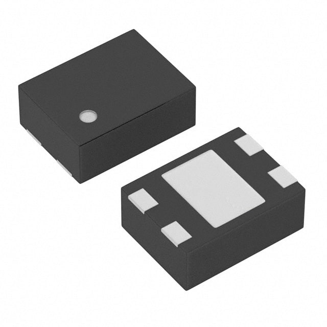
XC6118C09DGR-G is available in a small SOT-89 package.
Essence
The essence of XC6118C09DGR-G is its ability to provide stable and regulated voltage to electronic devices.
Packaging/Quantity
XC6118C09DGR-G is typically packaged in reels and comes in quantities of 3000 units per reel.
Specifications
- Input Voltage Range: 2.5V - 6.0V
- Output Voltage: 3.3V
- Dropout Voltage: 200mV (typical)
- Quiescent Current: 30µA (typical)
- Operating Temperature Range: -40°C to +85°C
Detailed Pin Configuration
XC6118C09DGR-G has three pins:
- VIN: Input voltage pin
- VOUT: Output voltage pin
- GND: Ground pin
Functional Features
- Low dropout voltage ensures efficient regulation even with low input voltages.
- High output voltage accuracy provides precise voltage regulation for sensitive components.
- Low quiescent current minimizes power consumption when the device is in standby mode.
- Thermal shutdown protection prevents damage due to excessive temperature.
- Short-circuit current limit protects the device from damage in case of a short circuit.
Advantages and Disadvantages
Advantages
- Reliable voltage regulation
- Compact size
- Low power consumption
- Wide operating temperature range
Disadvantages
- Limited output voltage options
- Sensitive to input voltage fluctuations
Working Principles
XC6118C09DGR-G operates based on the principle of a linear voltage regulator. It uses a pass transistor to regulate the output voltage by adjusting the resistance between the input and output pins. The internal circuitry monitors the input voltage and adjusts the pass transistor accordingly to maintain a stable output voltage.
Detailed Application Field Plans
XC6118C09DGR-G is commonly used in various electronic devices, including:
- Battery-powered devices
- Portable audio players
- IoT devices
- Wearable devices
- Automotive electronics
Detailed and Complete Alternative Models
Some alternative models that can be considered as alternatives to XC6118C09DGR-G are:
- LM1117-3.3
- LT1763-3.3
- MCP1700-3302E/TO
These models offer similar voltage regulation capabilities and can be suitable replacements depending on specific requirements.
In conclusion, XC6118C09DGR-G is a voltage regulator with low dropout voltage, high output voltage accuracy, and low quiescent current. It is commonly used in battery-powered devices, portable audio players, IoT devices, wearable devices, and automotive electronics. While it has limitations in terms of output voltage options and sensitivity to input voltage fluctuations, it provides reliable voltage regulation in a compact package.
技術ソリューションにおける XC6118C09DGR-G の適用に関連する 10 件の一般的な質問と回答をリストします。
Sure! Here are 10 common questions and answers related to the application of XC6118C09DGR-G in technical solutions:
Q: What is XC6118C09DGR-G? A: XC6118C09DGR-G is a voltage detector IC (integrated circuit) that monitors the power supply voltage and provides a reset signal when the voltage drops below a certain threshold.
Q: What is the operating voltage range of XC6118C09DGR-G? A: The operating voltage range of XC6118C09DGR-G is typically between 0.9V and 6.0V.
Q: How does XC6118C09DGR-G help in technical solutions? A: XC6118C09DGR-G helps ensure stable operation of electronic devices by monitoring the power supply voltage and generating a reset signal to prevent erratic behavior or data corruption during power fluctuations.
Q: Can XC6118C09DGR-G be used in battery-powered applications? A: Yes, XC6118C09DGR-G can be used in battery-powered applications as it has a low quiescent current consumption of typically 1.0µA, making it suitable for power-sensitive designs.
Q: What is the output type of XC6118C09DGR-G? A: XC6118C09DGR-G has an open-drain output, which means it can be connected to other devices with different voltage levels.
Q: What is the typical reset threshold voltage of XC6118C09DGR-G? A: The typical reset threshold voltage of XC6118C09DGR-G is 0.9V, but it can be adjusted using external resistors.
Q: Is XC6118C09DGR-G suitable for automotive applications? A: Yes, XC6118C09DGR-G is suitable for automotive applications as it meets the AEC-Q100 Grade 2 qualification standards.
Q: Can XC6118C09DGR-G be used in industrial control systems? A: Yes, XC6118C09DGR-G can be used in industrial control systems as it operates reliably in a wide temperature range (-40°C to +85°C) and has built-in hysteresis for noise immunity.
Q: Does XC6118C09DGR-G have any built-in delay time for the reset signal? A: No, XC6118C09DGR-G does not have a built-in delay time. The reset signal is generated immediately when the voltage drops below the threshold.
Q: Can XC6118C09DGR-G be used in space-constrained designs? A: Yes, XC6118C09DGR-G is available in a small SOT-25 package, making it suitable for space-constrained designs where board space is limited.
Please note that the answers provided here are general and may vary depending on specific datasheet specifications and application requirements.