

UCC37325DGN - English Editing Encyclopedia Entry
Product Overview
Category
UCC37325DGN belongs to the category of integrated circuits (ICs).
Use
This product is commonly used as a high-speed, dual-channel, low-side gate driver.
Characteristics
- High-speed switching capability
- Dual-channel design
- Low-side gate driving functionality
- Efficient power management
- Compact and versatile package
Package
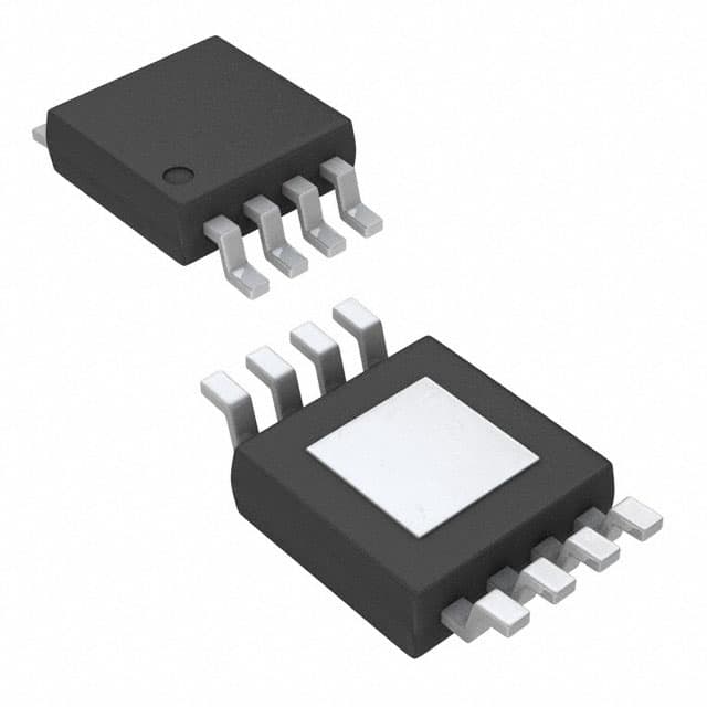
UCC37325DGN is available in a small-outline integrated circuit (SOIC) package.
Essence
The essence of UCC37325DGN lies in its ability to provide efficient and reliable gate driving for various applications.
Packaging/Quantity
This product is typically packaged in reels or tubes, with quantities varying based on customer requirements.
Specifications
- Supply voltage: 4.5V to 18V
- Output current: ±2A
- Rise/fall time: 10ns (typical)
- Operating temperature range: -40°C to +125°C
- Input logic compatibility: CMOS, TTL
Detailed Pin Configuration
UCC37325DGN features a 8-pin SOIC package with the following pin configuration:
- VDD - Power supply voltage
- IN1 - Input control signal for channel 1
- GND - Ground reference
- OUT1 - Output for channel 1
- VSS - Negative power supply voltage
- IN2 - Input control signal for channel 2
- GND - Ground reference
- OUT2 - Output for channel 2
Functional Features
- High-speed switching: Enables rapid response times in driving external devices.
- Dual-channel design: Allows independent control of two separate output channels.
- Low-side gate driving: Suitable for driving low-side switches in various applications.
- Efficient power management: Optimizes power consumption and reduces heat dissipation.
- Robust protection features: Built-in safeguards against overcurrent, overvoltage, and short circuits.
Advantages and Disadvantages
Advantages
- High-speed switching capability enhances system performance.
- Dual-channel design provides flexibility in driving multiple loads.
- Efficient power management reduces energy consumption.
- Robust protection features ensure reliable operation.
- Compact package size enables space-saving designs.
Disadvantages
- Limited output current may not be suitable for high-power applications.
- Restricted input logic compatibility may require additional level-shifting circuitry.
Working Principles
UCC37325DGN operates by receiving input control signals (IN1 and IN2) and generating corresponding output signals (OUT1 and OUT2) to drive external devices. The device utilizes internal circuitry to amplify and shape the input signals, enabling efficient gate driving of low-side switches. The high-speed switching capability ensures rapid response times, while the integrated protection features safeguard against potential faults.
Detailed Application Field Plans
UCC37325DGN finds extensive application in various fields, including but not limited to: - Motor control systems - Power electronics - Industrial automation - Automotive electronics - Renewable energy systems
Detailed and Complete Alternative Models
- UCC27324DGN
- UCC27325DGN
- UCC27326DGN
- UCC27327DGN
- UCC27328DGN
These alternative models offer similar functionality and characteristics, providing users with a range of options based on their specific requirements.
In conclusion, UCC37325DGN is a high-speed, dual-channel, low-side gate driver that offers efficient and reliable gate driving capabilities. Its compact package, robust protection features, and versatile applications make it a valuable component in various electronic systems.
Word count: 511
技術ソリューションにおける UCC37325DGN の適用に関連する 10 件の一般的な質問と回答をリストします。
Sure! Here are 10 common questions and answers related to the application of UCC37325DGN in technical solutions:
Q: What is UCC37325DGN? A: UCC37325DGN is a high-speed dual MOSFET driver IC used for driving power MOSFETs or IGBTs in various applications.
Q: What is the maximum operating voltage of UCC37325DGN? A: The maximum operating voltage of UCC37325DGN is typically 18V.
Q: What is the output current capability of UCC37325DGN? A: UCC37325DGN can source/sink up to 4A of peak current per channel.
Q: Can UCC37325DGN be used with both N-channel and P-channel MOSFETs? A: Yes, UCC37325DGN can be used with both N-channel and P-channel MOSFETs.
Q: What is the input voltage range of UCC37325DGN? A: The input voltage range of UCC37325DGN is typically from 2.5V to 18V.
Q: Does UCC37325DGN have built-in protection features? A: Yes, UCC37325DGN has built-in undervoltage lockout (UVLO) and thermal shutdown protection.
Q: What is the typical propagation delay of UCC37325DGN? A: The typical propagation delay of UCC37325DGN is around 15ns.
Q: Can UCC37325DGN operate at high temperatures? A: Yes, UCC37325DGN has a wide temperature range and can operate at temperatures up to 125°C.
Q: What is the purpose of the enable pin in UCC37325DGN? A: The enable pin allows for the control of the output stage, enabling or disabling the driver as needed.
Q: Can UCC37325DGN be used in motor control applications? A: Yes, UCC37325DGN can be used in motor control applications where high-speed switching of MOSFETs or IGBTs is required.
Please note that the answers provided here are general and may vary depending on specific datasheet specifications and application requirements.