

UCC27211DDAR
Product Overview
Category
UCC27211DDAR belongs to the category of integrated circuits (ICs).
Use
This product is commonly used in power management applications.
Characteristics
- High efficiency
- Low power consumption
- Fast switching speed
- Wide operating voltage range
Package
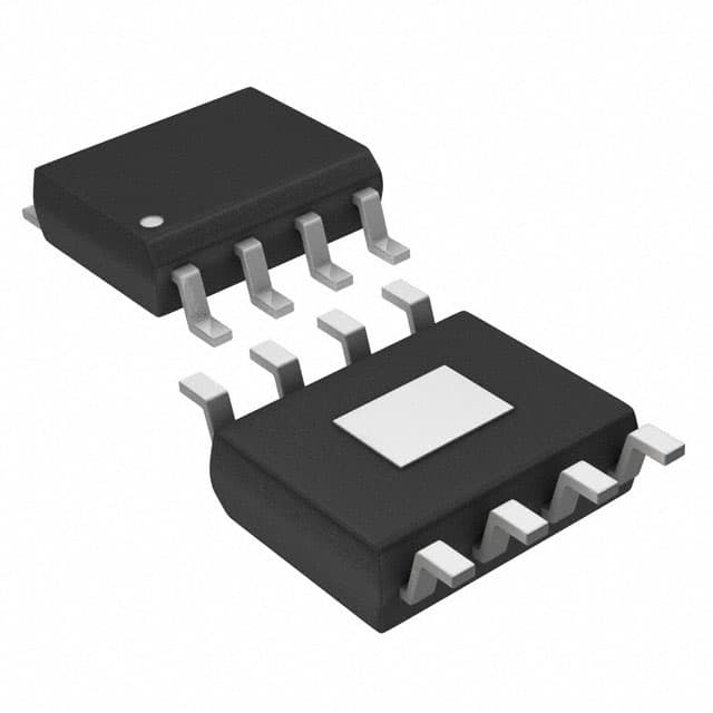
UCC27211DDAR is available in a small outline package (SOP) with 8 pins.
Essence
The essence of UCC27211DDAR lies in its ability to efficiently control and switch power in various electronic devices.
Packaging/Quantity
UCC27211DDAR is typically packaged in reels, with each reel containing a quantity of 2500 units.
Specifications
- Input Voltage Range: 4.5V to 18V
- Output Voltage Range: 0V to 18V
- Maximum Output Current: 2A
- Operating Temperature Range: -40°C to 125°C
- Switching Frequency: 1MHz
Detailed Pin Configuration
- VDD: Power supply input
- GND: Ground reference
- IN: Input pin for controlling the power switch
- OUT: Output pin connected to the load
- EN: Enable pin for turning the device on/off
- FB: Feedback pin for voltage regulation
- NC: No connection
- PGND: Power ground reference
Functional Features
- High-efficiency synchronous buck converter
- Integrated high-side and low-side power MOSFETs
- Adaptive dead-time control for improved efficiency
- Overcurrent protection
- Undervoltage lockout
- Thermal shutdown protection
Advantages and Disadvantages
Advantages
- High efficiency leads to reduced power loss
- Fast switching speed enables rapid response to load changes
- Wide operating voltage range allows for versatile applications
- Integrated power MOSFETs simplify circuit design
Disadvantages
- Limited maximum output current of 2A may not be suitable for high-power applications
- Requires careful thermal management due to the compact package size
Working Principles
UCC27211DDAR operates as a synchronous buck converter, converting a higher input voltage to a lower output voltage. It utilizes the integrated power MOSFETs to efficiently switch the power on and off. The device incorporates adaptive dead-time control to optimize efficiency and minimize power loss. Overcurrent protection, undervoltage lockout, and thermal shutdown features ensure safe operation.
Detailed Application Field Plans
UCC27211DDAR finds applications in various fields, including: 1. Power supplies for consumer electronics 2. LED lighting systems 3. Battery charging circuits 4. Motor control systems 5. Industrial automation equipment
Detailed and Complete Alternative Models
Some alternative models that can be considered as alternatives to UCC27211DDAR are: 1. UCC27212DDAR 2. UCC27213DDAR 3. UCC27214DDAR 4. UCC27215DDAR 5. UCC27216DDAR
These models offer similar functionality and characteristics, providing flexibility in choosing the most suitable option for specific applications.
Word count: 446 words
技術ソリューションにおける UCC27211DDAR の適用に関連する 10 件の一般的な質問と回答をリストします。
Sure! Here are 10 common questions and answers related to the application of UCC27211DDAR in technical solutions:
Q: What is UCC27211DDAR? A: UCC27211DDAR is a high-speed, dual-channel gate driver IC designed for driving power MOSFETs and IGBTs in various applications.
Q: What is the maximum operating voltage of UCC27211DDAR? A: The maximum operating voltage of UCC27211DDAR is typically 18V.
Q: Can UCC27211DDAR be used with both MOSFETs and IGBTs? A: Yes, UCC27211DDAR can be used to drive both power MOSFETs and IGBTs.
Q: What is the maximum output current capability of UCC27211DDAR? A: The maximum output current capability of UCC27211DDAR is typically 4A.
Q: Is UCC27211DDAR suitable for high-frequency switching applications? A: Yes, UCC27211DDAR is designed for high-speed operation and is suitable for high-frequency switching applications.
Q: Does UCC27211DDAR have built-in protection features? A: Yes, UCC27211DDAR includes various protection features such as undervoltage lockout (UVLO), overcurrent protection (OCP), and thermal shutdown.
Q: What is the input logic voltage level required for UCC27211DDAR? A: The input logic voltage level for UCC27211DDAR is compatible with standard CMOS or LSTTL logic levels, typically ranging from 3.3V to 15V.
Q: Can UCC27211DDAR be used in automotive applications? A: Yes, UCC27211DDAR is suitable for automotive applications and meets the necessary automotive standards.
Q: What is the typical propagation delay of UCC27211DDAR? A: The typical propagation delay of UCC27211DDAR is around 25ns.
Q: Is UCC27211DDAR available in different package options? A: Yes, UCC27211DDAR is available in various package options, including SOIC-8 and VSSOP-8.
Please note that the answers provided here are general and may vary depending on specific datasheet specifications and application requirements.