

UCC2583QG3 - English Editing Encyclopedia Entry
Product Overview
Category
UCC2583QG3 belongs to the category of integrated circuits (ICs).
Use
This IC is commonly used in power management applications.
Characteristics
- High efficiency
- Low power consumption
- Compact size
- Wide input voltage range
Package
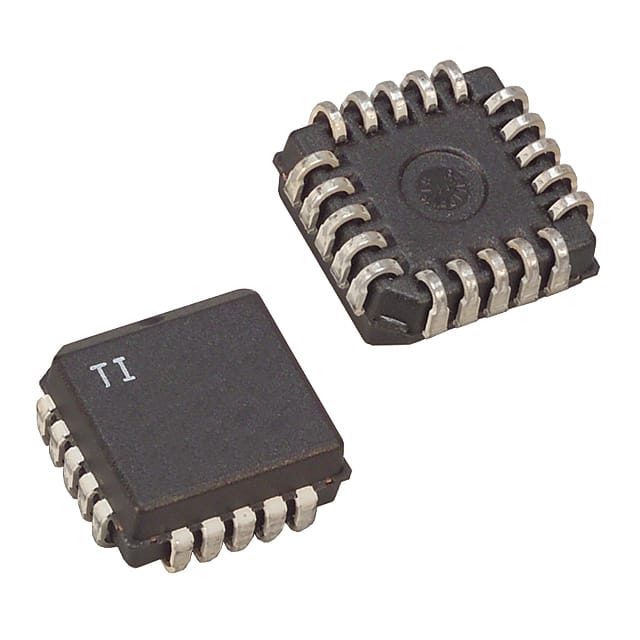
UCC2583QG3 is available in a small outline package (SOP) or a thin shrink small outline package (TSSOP).
Essence
The essence of UCC2583QG3 lies in its ability to efficiently regulate and control power in various electronic devices.
Packaging/Quantity
UCC2583QG3 is typically packaged in reels or tubes, with quantities varying depending on the manufacturer's specifications.
Specifications
- Input Voltage Range: 4.5V to 40V
- Output Voltage Range: 1.23V to 37V
- Output Current: Up to 2A
- Switching Frequency: Adjustable up to 500kHz
- Operating Temperature Range: -40°C to 125°C
Detailed Pin Configuration
UCC2583QG3 features a standard pin configuration with the following pins:
- VIN: Input voltage pin
- GND: Ground pin
- FB: Feedback pin for output voltage regulation
- COMP: Compensation pin for stability control
- EN: Enable pin for turning the IC on/off
- VOUT: Output voltage pin
- SW: Switching pin for power regulation
- SS/TR: Soft-start/Tracking pin for gradual power-up
Functional Features
- Wide Input Voltage Range: Allows compatibility with various power sources.
- Adjustable Output Voltage: Enables flexibility in meeting specific device requirements.
- High Efficiency: Minimizes power loss and maximizes energy utilization.
- Current Limit Protection: Safeguards against excessive current flow, preventing damage to the IC and connected devices.
- Soft-Start Function: Ensures a smooth power-up sequence, reducing stress on components.
Advantages and Disadvantages
Advantages
- High efficiency leads to reduced power consumption.
- Compact size allows for space-saving designs.
- Wide input voltage range enhances versatility.
- Current limit protection ensures device safety.
Disadvantages
- Limited output current capacity may not be suitable for high-power applications.
- Higher cost compared to some alternative models.
Working Principles
UCC2583QG3 operates based on a switching regulator principle. It utilizes a control circuit to regulate the output voltage by adjusting the duty cycle of the internal power switch. This enables efficient conversion of the input voltage to the desired output voltage while minimizing power loss.
Detailed Application Field Plans
UCC2583QG3 finds application in various fields, including but not limited to: - Power supplies for consumer electronics - Industrial automation systems - Automotive electronics - LED lighting systems - Battery charging circuits
Detailed and Complete Alternative Models
Some alternative models that can be considered as alternatives to UCC2583QG3 are: - LM2576-ADJ - LT1073 - TPS5430
These models offer similar functionality and can be used as substitutes depending on specific requirements.
In conclusion, UCC2583QG3 is a versatile integrated circuit used for power management applications. Its high efficiency, compact size, and wide input voltage range make it suitable for various electronic devices. While it has limitations in terms of output current capacity and cost, its advantages outweigh these disadvantages. With its reliable performance and numerous applications, UCC2583QG3 is a valuable component in the field of power management.
技術ソリューションにおける UCC2583QG3 の適用に関連する 10 件の一般的な質問と回答をリストします。
Sure! Here are 10 common questions and answers related to the application of UCC2583QG3 in technical solutions:
Question: What is UCC2583QG3?
Answer: UCC2583QG3 is a high-performance synchronous rectifier controller IC used in power supply applications.Question: What is the purpose of UCC2583QG3?
Answer: UCC2583QG3 is designed to control the synchronous rectification process, improving efficiency and reducing power losses in power supply designs.Question: What are the key features of UCC2583QG3?
Answer: Some key features include adaptive dead-time control, programmable soft-start, overcurrent protection, and thermal shutdown.Question: How does UCC2583QG3 improve power supply efficiency?
Answer: UCC2583QG3 enables synchronous rectification, which reduces power losses by replacing diode rectifiers with low-resistance MOSFETs.Question: Can UCC2583QG3 be used in both buck and boost converter topologies?
Answer: Yes, UCC2583QG3 can be used in both buck and boost converter topologies, making it versatile for various power supply designs.Question: What is adaptive dead-time control, and why is it important?
Answer: Adaptive dead-time control adjusts the timing between the turn-off of one MOSFET and the turn-on of the other, minimizing shoot-through current and improving overall efficiency.Question: Does UCC2583QG3 have any protection features?
Answer: Yes, UCC2583QG3 has built-in overcurrent protection and thermal shutdown to safeguard the power supply from excessive current or temperature.Question: Can UCC2583QG3 operate at high switching frequencies?
Answer: Yes, UCC2583QG3 is designed to operate at high switching frequencies, making it suitable for applications that require fast response times.Question: Is UCC2583QG3 easy to integrate into existing power supply designs?
Answer: Yes, UCC2583QG3 comes in a compact package and requires minimal external components, making it relatively easy to integrate into existing designs.Question: Are there any application notes or reference designs available for UCC2583QG3?
Answer: Yes, Texas Instruments provides application notes and reference designs that can help users understand and implement UCC2583QG3 in their technical solutions.
Please note that the answers provided here are general and may vary depending on specific design requirements and application scenarios.