

TPS22906YZVR
Product Overview
Category
The TPS22906YZVR belongs to the category of power management integrated circuits (PMICs).
Use
This PMIC is primarily used for managing power in electronic devices, specifically for load switching applications.
Characteristics
- Low on-resistance
- Fast switching speed
- Wide input voltage range
- Overcurrent and overtemperature protection
- Low quiescent current
Package
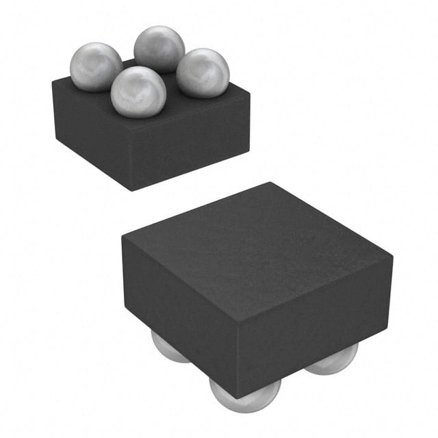
The TPS22906YZVR is available in a small 4-ball wafer chip scale package (WCSP), measuring 0.8mm x 0.8mm.
Essence
The essence of the TPS22906YZVR lies in its ability to efficiently control power flow in electronic devices, ensuring optimal performance and protection against potential damage.
Packaging/Quantity
This PMIC is typically packaged in reels, with each reel containing 3000 units.
Specifications
- Input Voltage Range: 1.5V to 5.5V
- On-Resistance: 30mΩ (typical)
- Quiescent Current: 0.1μA (typical)
- Operating Temperature Range: -40°C to 85°C
Detailed Pin Configuration
The TPS22906YZVR has the following pin configuration:
- VIN: Input voltage pin
- EN: Enable pin
- GND: Ground pin
- VOUT: Output voltage pin
Functional Features
- Load switching capability
- Power sequencing support
- Undervoltage lockout (UVLO) protection
- Thermal shutdown protection
- ESD protection
Advantages and Disadvantages
Advantages
- Low on-resistance ensures minimal power loss
- Fast switching speed improves overall device performance
- Wide input voltage range allows compatibility with various power sources
- Overcurrent and overtemperature protection safeguards against potential damage
- Low quiescent current minimizes power consumption
Disadvantages
- Limited output current capacity
- Small package size may pose challenges during assembly and soldering processes
Working Principles
The TPS22906YZVR operates by controlling the flow of power from the input voltage (VIN) to the output voltage (VOUT) based on the enable signal (EN). When the enable pin is high, the PMIC allows power to flow from VIN to VOUT. Conversely, when the enable pin is low, the power flow is interrupted.
Detailed Application Field Plans
The TPS22906YZVR finds applications in various electronic devices that require efficient load switching and power management. Some specific application fields include:
- Mobile devices: Smartphones, tablets, portable gaming consoles.
- Wearable devices: Smartwatches, fitness trackers, augmented reality glasses.
- Internet of Things (IoT) devices: Home automation systems, smart sensors, connected appliances.
- Portable electronics: MP3 players, digital cameras, handheld gaming devices.
Detailed and Complete Alternative Models
- TPS22907YZVR: Similar to TPS22906YZVR, but with higher output current capacity.
- TPS22908YZVR: Similar to TPS22906YZVR, but with additional features such as adjustable output voltage.
These alternative models provide similar functionality to the TPS22906YZVR, catering to different requirements and specifications.
In conclusion, the TPS22906YZVR is a power management integrated circuit designed for load switching applications. Its low on-resistance, fast switching speed, and wide input voltage range make it suitable for various electronic devices. While it has limitations in terms of output current capacity and package size, its advantages outweigh the disadvantages. The working principle involves controlling power flow based on the enable signal. It finds applications in mobile devices, wearables, IoT devices, and portable electronics. Alternative models such as TPS22907YZVR and TPS22908YZVR offer similar functionality with additional features.
技術ソリューションにおける TPS22906YZVR の適用に関連する 10 件の一般的な質問と回答をリストします。
Sure! Here are 10 common questions and answers related to the application of TPS22906YZVR:
Q: What is TPS22906YZVR? A: TPS22906YZVR is a low-voltage, ultra-low Rds(on) load switch with an integrated power-good output.
Q: What is the typical input voltage range for TPS22906YZVR? A: The typical input voltage range for TPS22906YZVR is from 0.75V to 5.5V.
Q: What is the maximum continuous current that TPS22906YZVR can handle? A: TPS22906YZVR can handle a maximum continuous current of 2A.
Q: Can TPS22906YZVR be used in battery-powered applications? A: Yes, TPS22906YZVR is suitable for battery-powered applications due to its low quiescent current and low shutdown current.
Q: Does TPS22906YZVR have overcurrent protection? A: Yes, TPS22906YZVR has built-in overcurrent protection to prevent damage to the load.
Q: Can TPS22906YZVR be used in hot-swapping applications? A: Yes, TPS22906YZVR supports hot swapping, allowing for safe insertion and removal of loads while the system is powered.
Q: What is the power-good output feature of TPS22906YZVR? A: The power-good output of TPS22906YZVR provides a signal indicating when the output voltage is within regulation limits.
Q: Is TPS22906YZVR compatible with both digital and analog signals? A: Yes, TPS22906YZVR is compatible with both digital and analog signals, making it versatile for various applications.
Q: Can TPS22906YZVR be used in low-power standby mode? A: Yes, TPS22906YZVR has a low quiescent current of typically 1µA, making it suitable for low-power standby mode.
Q: What is the thermal shutdown feature of TPS22906YZVR? A: The thermal shutdown feature of TPS22906YZVR protects the device from overheating by shutting down when the junction temperature exceeds a certain threshold.
Please note that these answers are general and may vary depending on the specific application and implementation of TPS22906YZVR.