

SN75LVCP412ARTJR
Product Overview
- Category: Integrated Circuit
- Use: Signal Conditioning and Data Transmission
- Characteristics: Low Voltage Differential Signaling (LVDS) Serializer/Deserializer (SerDes)
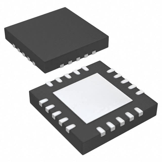
- Package: 32-pin QFN (Quad Flat No-Lead)
- Essence: Converts parallel data into serial data and vice versa for high-speed data transmission
- Packaging/Quantity: Tape and Reel, 2500 units per reel
Specifications
- Supply Voltage Range: 3.0V to 3.6V
- Operating Temperature Range: -40°C to +85°C
- Data Rate: Up to 1.5 Gbps
- Number of Channels: 4
- Input/Output Interface: LVCMOS/LVTTL
- Power Dissipation: 200mW (typical)
Detailed Pin Configuration
The SN75LVCP412ARTJR has a total of 32 pins. The pin configuration is as follows:
- VCCO1: LVCMOS/LVTTL Output Power Supply
- O1P: LVCMOS/LVTTL Output Positive Data Channel 1
- O1N: LVCMOS/LVTTL Output Negative Data Channel 1
- VCCO2: LVCMOS/LVTTL Output Power Supply
- O2P: LVCMOS/LVTTL Output Positive Data Channel 2
- O2N: LVCMOS/LVTTL Output Negative Data Channel 2
- VCCO3: LVCMOS/LVTTL Output Power Supply
- O3P: LVCMOS/LVTTL Output Positive Data Channel 3
- O3N: LVCMOS/LVTTL Output Negative Data Channel 3
- VCCO4: LVCMOS/LVTTL Output Power Supply
- O4P: LVCMOS/LVTTL Output Positive Data Channel 4
- O4N: LVCMOS/LVTTL Output Negative Data Channel 4
- VCCO5: LVCMOS/LVTTL Output Power Supply
- GND: Ground
- VCCO6: LVCMOS/LVTTL Output Power Supply
- I1P: LVCMOS/LVTTL Input Positive Data Channel 1
- I1N: LVCMOS/LVTTL Input Negative Data Channel 1
- VCCO7: LVCMOS/LVTTL Output Power Supply
- I2P: LVCMOS/LVTTL Input Positive Data Channel 2
- I2N: LVCMOS/LVTTL Input Negative Data Channel 2
- VCCO8: LVCMOS/LVTTL Output Power Supply
- I3P: LVCMOS/LVTTL Input Positive Data Channel 3
- I3N: LVCMOS/LVTTL Input Negative Data Channel 3
- VCCO9: LVCMOS/LVTTL Output Power Supply
- I4P: LVCMOS/LVTTL Input Positive Data Channel 4
- I4N: LVCMOS/LVTTL Input Negative Data Channel 4
- VCCO10: LVCMOS/LVTTL Output Power Supply
- GND: Ground
- VCCO11: LVCMOS/LVTTL Output Power Supply
- GND: Ground
- VCCO12: LVCMOS/LVTTL Output Power Supply
- GND: Ground
Functional Features
- Converts parallel data into serial data and vice versa
- Supports high-speed data transmission up to 1.5 Gbps
- LVCMOS/LVTTL compatible input and output interface
- Low voltage differential signaling for noise immunity
Advantages and Disadvantages
Advantages: - High-speed data transmission capability - Low power consumption - Noise immunity due to LVDS technology
Disadvantages: - Limited number of channels (4 in this case) - Requires LVCMOS/LVTTL compatible devices for interfacing
Working Principles
The SN75LVCP412ARTJR is a Serializer/Deserializer (SerDes) IC that converts parallel data into serial data and vice versa. It utilizes Low Voltage Differential Signaling (LVDS) technology, which provides high-speed data transmission with low power consumption and noise immunity. The IC receives parallel data through its input channels and converts it into a serial data stream. Similarly, it can receive a serial data stream and convert it back into parallel data. The LVCMOS/LVTTL compatible interface allows easy integration with other digital devices.
Detailed Application Field Plans
The SN75LVCP412ARTJR is commonly used in various applications requiring high-speed data transmission and signal conditioning. Some of the application fields
技術ソリューションにおける SN75LVCP412ARTJR の適用に関連する 10 件の一般的な質問と回答をリストします。
Sure! Here are 10 common questions and answers related to the application of SN75LVCP412ARTJR in technical solutions:
Q: What is SN75LVCP412ARTJR? A: SN75LVCP412ARTJR is a high-speed differential line driver and receiver designed for applications requiring ultra-low power consumption and high data rates.
Q: What is the operating voltage range of SN75LVCP412ARTJR? A: The operating voltage range of SN75LVCP412ARTJR is from 3.0V to 3.6V.
Q: What is the maximum data rate supported by SN75LVCP412ARTJR? A: SN75LVCP412ARTJR supports a maximum data rate of 12 Gbps.
Q: Can SN75LVCP412ARTJR be used in point-to-point or multipoint applications? A: Yes, SN75LVCP412ARTJR can be used in both point-to-point and multipoint applications.
Q: Does SN75LVCP412ARTJR support hot-plugging capability? A: Yes, SN75LVCP412ARTJR supports hot-plugging capability, allowing devices to be connected or disconnected while the system is powered on.
Q: What is the typical power consumption of SN75LVCP412ARTJR? A: The typical power consumption of SN75LVCP412ARTJR is very low, typically around 20 mW.
Q: Is SN75LVCP412ARTJR compatible with different transmission media? A: Yes, SN75LVCP412ARTJR is compatible with various transmission media such as FR-4, stripline, and microstrip.
Q: Can SN75LVCP412ARTJR be used in high-speed data communication applications? A: Yes, SN75LVCP412ARTJR is specifically designed for high-speed data communication applications, including Ethernet, USB, and PCIe.
Q: Does SN75LVCP412ARTJR have built-in protection features? A: Yes, SN75LVCP412ARTJR has built-in protection features such as overvoltage protection and thermal shutdown.
Q: What package does SN75LVCP412ARTJR come in? A: SN75LVCP412ARTJR is available in a small 32-pin QFN package, making it suitable for space-constrained designs.
Please note that these answers are general and may vary depending on the specific application and requirements. It is always recommended to refer to the datasheet and consult with the manufacturer for detailed information.