

SN74SSTV32852ZKFR
Product Overview
Category
The SN74SSTV32852ZKFR belongs to the category of integrated circuits (ICs).
Use
This IC is commonly used in electronic devices for signal transmission and processing.
Characteristics
- High-speed operation
- Low power consumption
- Wide operating voltage range
- Robust design for reliable performance
Package
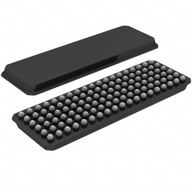
The SN74SSTV32852ZKFR is available in a compact surface-mount package.
Essence
This IC serves as a key component in various electronic systems, enabling efficient signal transmission and processing.
Packaging/Quantity
The SN74SSTV32852ZKFR is typically packaged in reels or tubes, with varying quantities depending on customer requirements.
Specifications
- Operating Voltage: 2.3V - 3.6V
- Operating Temperature Range: -40°C to +85°C
- Number of Pins: 56
- Logic Family: SSTL_18
Detailed Pin Configuration
The SN74SSTV32852ZKFR features 56 pins, each serving a specific function within the circuit. The pin configuration is as follows:
- Pin 1: VDDA
- Pin 2: VSSA
- Pin 3: DQA0
- Pin 4: DQA1
- Pin 5: DQA2
- Pin 6: DQA3
- Pin 7: DQA4
- Pin 8: DQA5
- Pin 9: DQA6
- Pin 10: DQA7
- Pin 11: DQA8
- Pin 12: DQA9
- Pin 13: DQA10
- Pin 14: DQA11
- Pin 15: DQA12
- Pin 16: DQA13
- Pin 17: DQA14
- Pin 18: DQA15
- Pin 19: VREF
- Pin 20: VDDQ
- Pin 21: VSSQ
- Pin 22: DQB0
- Pin 23: DQB1
- Pin 24: DQB2
- Pin 25: DQB3
- Pin 26: DQB4
- Pin 27: DQB5
- Pin 28: DQB6
- Pin 29: DQB7
- Pin 30: DQB8
- Pin 31: DQB9
- Pin 32: DQB10
- Pin 33: DQB11
- Pin 34: DQB12
- Pin 35: DQB13
- Pin 36: DQB14
- Pin 37: DQB15
- Pin 38: VDDQ
- Pin 39: VSSQ
- Pin 40: VDDA
- Pin 41: VSSA
- Pin 42: DQA16
- Pin 43: DQA17
- Pin 44: DQA18
- Pin 45: DQA19
- Pin 46: DQA20
- Pin 47: DQA21
- Pin 48: DQA22
- Pin 49: DQA23
- Pin 50: DQA24
- Pin 51: DQA25
- Pin 52: DQA26
- Pin 53: DQA27
- Pin 54: DQA28
- Pin 55: DQA29
- Pin 56: DQA30
Functional Features
- High-speed data transmission
- Low power consumption
- Built-in error detection and correction mechanisms
- Support for various communication protocols
- Flexible configuration options
Advantages and Disadvantages
Advantages
- High-speed operation enables efficient data processing
- Low power consumption contributes to energy efficiency
- Robust design ensures reliable performance in demanding environments
- Versatile functionality supports diverse applications
Disadvantages
- Complex pin configuration may require careful attention during circuit design
- Limited availability of alternative models from other manufacturers
Working Principles
The SN74SSTV32852ZKFR operates based on advanced semiconductor technology. It utilizes a combination of logic gates, flip-flops, and other components to process and transmit digital signals. The IC follows predefined algorithms and protocols to ensure accurate and reliable data transfer.
Detailed Application Field Plans
The SN74SSTV32852ZKFR finds extensive use in various
技術ソリューションにおける SN74SSTV32852ZKFR の適用に関連する 10 件の一般的な質問と回答をリストします。
Sure! Here are 10 common questions and answers related to the application of SN74SSTV32852ZKFR in technical solutions:
Q: What is SN74SSTV32852ZKFR? A: SN74SSTV32852ZKFR is a specific model of integrated circuit (IC) designed for high-speed data transmission and signal conditioning.
Q: What are the key features of SN74SSTV32852ZKFR? A: Some key features include 32-bit wide bus, voltage translation, hot swap capability, and support for various signaling standards like LVCMOS, LVTTL, and SSTL.
Q: In what applications can SN74SSTV32852ZKFR be used? A: SN74SSTV32852ZKFR can be used in various applications such as networking equipment, telecommunications systems, data centers, and high-speed computing.
Q: How does SN74SSTV32852ZKFR help in signal conditioning? A: SN74SSTV32852ZKFR provides voltage level shifting and impedance matching capabilities, ensuring proper signal integrity and compatibility between different devices or subsystems.
Q: Can SN74SSTV32852ZKFR handle multiple voltage levels? A: Yes, SN74SSTV32852ZKFR supports voltage translation between different voltage domains, making it suitable for mixed-voltage systems.
Q: Does SN74SSTV32852ZKFR support hot swapping of devices? A: Yes, SN74SSTV32852ZKFR has built-in hot swap circuitry that allows for safe insertion and removal of devices without disrupting the system operation.
Q: What signaling standards are supported by SN74SSTV32852ZKFR? A: SN74SSTV32852ZKFR supports various signaling standards such as LVCMOS, LVTTL, and SSTL, making it versatile for different interface requirements.
Q: What is the maximum data rate supported by SN74SSTV32852ZKFR? A: SN74SSTV32852ZKFR can support data rates up to several gigabits per second (Gbps), depending on the specific application and system configuration.
Q: Are there any special considerations for PCB layout when using SN74SSTV32852ZKFR? A: Yes, it is recommended to follow the manufacturer's guidelines for proper PCB layout, including signal routing, power supply decoupling, and thermal management.
Q: Where can I find more information about SN74SSTV32852ZKFR? A: You can refer to the datasheet provided by the manufacturer or visit their official website for detailed information about SN74SSTV32852ZKFR, including specifications, application notes, and reference designs.
Please note that the answers provided here are general and may vary based on specific requirements and use cases. It is always recommended to consult the manufacturer's documentation for accurate and up-to-date information.