

SN74LVC32374AGKER
Product Overview
- Category: Integrated Circuit (IC)
- Use: Flip-Flop
- Characteristics: Low-voltage, high-speed, 32-bit D-type flip-flop with 3-state outputs
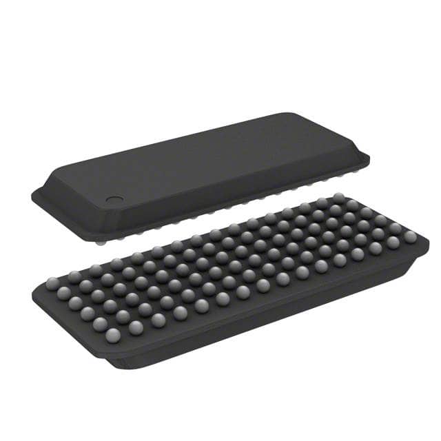
- Package: 48-pin TSSOP
- Essence: Reliable and efficient storage element for digital data
- Packaging/Quantity: Available in reels of 2500 units
Specifications
The SN74LVC32374AGKER is a 32-bit D-type flip-flop with 3-state outputs. It operates at low voltage levels and offers high-speed performance. The IC is designed to store digital data reliably and efficiently.
Key specifications include:
- Supply Voltage Range: 1.65V to 3.6V
- High-Speed Operation: Up to 200MHz
- Output Drive Capability: ±24mA
- Operating Temperature Range: -40°C to +85°C
- Input/Output Compatibility: TTL, CMOS
Detailed Pin Configuration
The SN74LVC32374AGKER has a total of 48 pins. The pin configuration is as follows:
- OE (Output Enable) 1
- Q0 (Output) 0
- D0 (Data) 0
- D1 (Data) 1
- Q1 (Output) 1
- GND (Ground)
- D2 (Data) 2
- Q2 (Output) 2
- D3 (Data) 3
- Q3 (Output) 3
- VCC (Power Supply)
- D4 (Data) 4
- Q4 (Output) 4
- D5 (Data) 5
- Q5 (Output) 5
- D6 (Data) 6
- Q6 (Output) 6
- D7 (Data) 7
- Q7 (Output) 7
- GND (Ground)
- D8 (Data) 8
- Q8 (Output) 8
- D9 (Data) 9
- Q9 (Output) 9
- D10 (Data) 10
- Q10 (Output) 10
- D11 (Data) 11
- Q11 (Output) 11
- VCC (Power Supply)
- D12 (Data) 12
- Q12 (Output) 12
- D13 (Data) 13
- Q13 (Output) 13
- D14 (Data) 14
- Q14 (Output) 14
- D15 (Data) 15
- Q15 (Output) 15
- GND (Ground)
- D16 (Data) 16
- Q16 (Output) 16
- D17 (Data) 17
- Q17 (Output) 17
- D18 (Data) 18
- Q18 (Output) 18
- D19 (Data) 19
- Q19 (Output) 19
- VCC (Power Supply)
- OE (Output Enable) 2
Functional Features
The SN74LVC32374AGKER offers the following functional features:
- 32-bit Storage: It can store digital data in its flip-flop registers.
- 3-State Outputs: The IC provides three-state outputs, allowing multiple devices to share a common bus without interference.
- Low-Voltage Operation: It operates at low voltage levels, making it suitable for battery-powered applications.
- High-Speed Performance: With a maximum operating frequency of 200MHz, it can handle high-speed data transfers efficiently.
Advantages and Disadvantages
Advantages:
- Reliable Data Storage: The flip-flop design ensures reliable storage of digital data.
- Compatibility: It is compatible with both TTL and CMOS logic levels.
- Low Power Consumption: The IC operates at low voltage levels, resulting in lower power consumption.
- High-Speed Operation: It can handle high-speed data transfers effectively.
Disadvantages:
- Limited Output Drive Capability: The output drive capability of ±24mA may not be sufficient for certain applications requiring higher current.
Working Principles
The SN74LVC32374AGKER operates based on the principles of D-type flip-flops. It stores digital data in its registers using clock signals. The input data is latched into the flip-flops on the rising edge of the clock signal. The stored data can be accessed through the output pins when the output enable (OE) signal is active.
Detailed Application Field Plans
The SN
技術ソリューションにおける SN74LVC32374AGKER の適用に関連する 10 件の一般的な質問と回答をリストします。
Sure! Here are 10 common questions and answers related to the application of SN74LVC32374AGKER:
Q: What is SN74LVC32374AGKER? A: SN74LVC32374AGKER is a 32-bit D-type flip-flop with 3-state outputs, designed for low-voltage (3.3V) applications.
Q: What are the key features of SN74LVC32374AGKER? A: Some key features include 3.3V operation, 32-bit flip-flop with 3-state outputs, and compatibility with various logic families.
Q: What is the maximum operating frequency of SN74LVC32374AGKER? A: The maximum operating frequency of SN74LVC32374AGKER is typically around 200 MHz.
Q: Can SN74LVC32374AGKER be used in both input and output applications? A: Yes, SN74LVC32374AGKER can be used as both an input and output device, depending on the specific requirements of your design.
Q: How many inputs and outputs does SN74LVC32374AGKER have? A: SN74LVC32374AGKER has 32 inputs and 32 outputs, making it suitable for handling large data sets.
Q: What is the power supply voltage range for SN74LVC32374AGKER? A: The power supply voltage range for SN74LVC32374AGKER is typically between 2.7V and 3.6V.
Q: Is SN74LVC32374AGKER compatible with other logic families? A: Yes, SN74LVC32374AGKER is compatible with various logic families, including TTL, CMOS, and LVCMOS.
Q: Can SN74LVC32374AGKER be used in high-speed applications? A: Yes, SN74LVC32374AGKER is designed to operate at relatively high speeds, making it suitable for many high-speed applications.
Q: What is the output drive strength of SN74LVC32374AGKER? A: The output drive strength of SN74LVC32374AGKER is typically around 12 mA, allowing it to drive moderate loads.
Q: Are there any specific application notes or reference designs available for SN74LVC32374AGKER? A: Yes, Texas Instruments provides application notes and reference designs that can help you understand and implement SN74LVC32374AGKER in your technical solutions.
Please note that these answers are general and may vary depending on the specific datasheet and manufacturer's recommendations for SN74LVC32374AGKER.