

SN74LVC2G157YEPR
Product Overview
- Category: Integrated Circuit (IC)
- Use: Logic Multiplexer/Demultiplexer
- Characteristics: Low-voltage, high-speed, dual 2-input multiplexer/demultiplexer
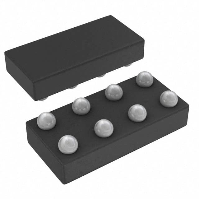
- Package: 8-pin VSSOP (Very Small Outline Package)
- Essence: A versatile IC that allows for efficient data routing and selection in digital circuits
- Packaging/Quantity: Available in tape and reel packaging, with a quantity of 2500 units per reel
Specifications
- Supply Voltage Range: 1.65V to 5.5V
- Input Voltage Range: 0V to VCC
- Output Voltage Range: 0V to VCC
- High-Level Input Voltage: 0.7 x VCC to VCC
- Low-Level Input Voltage: 0V to 0.3 x VCC
- High-Level Output Voltage: 0.9 x VCC to VCC
- Low-Level Output Voltage: 0V to 0.1 x VCC
- Maximum Operating Frequency: 100 MHz
- Propagation Delay: 4.6 ns (typical)
Detailed Pin Configuration
The SN74LVC2G157YEPR has the following pin configuration:
- A Input (Pin 1)
- B Input (Pin 2)
- Y Output (Pin 3)
- GND (Ground) (Pin 4)
- Y Output (Pin 5)
- B Input (Pin 6)
- A Input (Pin 7)
- VCC (Power Supply) (Pin 8)
Functional Features
- Dual 2-input multiplexer/demultiplexer functionality
- Low-voltage operation suitable for battery-powered devices
- High-speed operation for efficient data processing
- Schmitt-trigger inputs for improved noise immunity
- 3-state outputs for flexible data routing
Advantages and Disadvantages
Advantages: - Versatile functionality as both a multiplexer and demultiplexer - Low-voltage operation extends battery life in portable devices - High-speed operation enables efficient data processing - Schmitt-trigger inputs provide robustness against noise - 3-state outputs allow for flexible data routing
Disadvantages: - Limited number of input/output channels (dual 2-input) - Propagation delay may impact timing-sensitive applications - Not suitable for high-voltage applications (limited to 5.5V)
Working Principles
The SN74LVC2G157YEPR operates by selectively routing or demultiplexing digital signals based on the control inputs. The A and B inputs determine which data input is connected to the output, controlled by the logic levels applied to these pins. The output can be enabled or disabled using the G (Gating) input. When the G input is low, the outputs are in a high-impedance state.
Detailed Application Field Plans
The SN74LVC2G157YEPR finds application in various fields, including:
- Data communication systems: Used for data routing and selection in multiplexed communication channels.
- Consumer electronics: Enables efficient signal routing in audio/video equipment, gaming consoles, and remote controls.
- Automotive electronics: Facilitates data selection and routing in automotive infotainment systems and control modules.
- Industrial automation: Allows for efficient data routing in PLCs (Programmable Logic Controllers) and industrial control systems.
- Medical devices: Used for data selection and routing in medical imaging equipment and patient monitoring systems.
Detailed and Complete Alternative Models
- SN74LVC2G157DCUR: Similar dual 2-input multiplexer/demultiplexer IC in a 8-pin VSSOP package.
- SN74LVC2G157DCKR: Dual 2-input multiplexer/demultiplexer IC in a 8-pin SC70 package.
- SN74LVC2G157DBVR: Dual 2-input multiplexer/demultiplexer IC in a 6-pin SOT-23 package.
These alternative models offer similar functionality and characteristics to the SN74LVC2G157YEPR, providing flexibility in choosing the most suitable option for specific applications.
Word count: 468 words
技術ソリューションにおける SN74LVC2G157YEPR の適用に関連する 10 件の一般的な質問と回答をリストします。
Sure! Here are 10 common questions and answers related to the application of SN74LVC2G157YEPR in technical solutions:
Q: What is the SN74LVC2G157YEPR? A: The SN74LVC2G157YEPR is a dual 2-input multiplexer/demultiplexer IC (Integrated Circuit) manufactured by Texas Instruments.
Q: What is the purpose of the SN74LVC2G157YEPR? A: The purpose of this IC is to provide multiplexing and demultiplexing functionality, allowing for the selection of one of two input signals or the distribution of one input signal to two outputs.
Q: What is the operating voltage range of the SN74LVC2G157YEPR? A: The operating voltage range of this IC is typically between 1.65V and 5.5V.
Q: What is the maximum data rate supported by the SN74LVC2G157YEPR? A: The maximum data rate supported by this IC is typically 400 Mbps (megabits per second).
Q: How many channels does the SN74LVC2G157YEPR have? A: The SN74LVC2G157YEPR has two independent channels, each with its own 2-input multiplexer/demultiplexer.
Q: What is the package type of the SN74LVC2G157YEPR? A: The SN74LVC2G157YEPR is available in a standard 8-pin VSSOP (Very Small Outline Package) package.
Q: Can the SN74LVC2G157YEPR be used in both digital and analog applications? A: Yes, the SN74LVC2G157YEPR can be used in both digital and analog applications, as it supports a wide voltage range.
Q: What is the power supply current consumption of the SN74LVC2G157YEPR? A: The power supply current consumption of this IC is typically around 1.5 mA (milliamperes) per channel.
Q: Does the SN74LVC2G157YEPR have any built-in protection features? A: Yes, the SN74LVC2G157YEPR has built-in ESD (Electrostatic Discharge) protection, which helps safeguard against damage from static electricity.
Q: Can the SN74LVC2G157YEPR be cascaded to increase the number of input/output channels? A: Yes, multiple SN74LVC2G157YEPR ICs can be cascaded together to increase the number of input/output channels in a system.