

SN74LVC1G19DRLR
Product Overview
- Category: Integrated Circuit (IC)
- Use: Logic Gate
- Characteristics: Single 2-input AND gate with Schmitt-trigger inputs
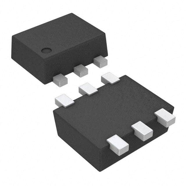
- Package: SOT-23-5
- Essence: High-speed CMOS technology
- Packaging/Quantity: Tape and Reel, 3000 pieces per reel
Specifications
- Supply Voltage Range: 1.65V to 5.5V
- Input Voltage Range: 0V to VCC
- Output Voltage Range: 0V to VCC
- Operating Temperature Range: -40°C to +85°C
- Propagation Delay: 3.8ns (typical) at 3.3V
- Quiescent Current: 10μA (maximum) at 3.3V
Detailed Pin Configuration
The SN74LVC1G19DRLR has a total of 5 pins:
- Pin 1: Input A
- Pin 2: Input B
- Pin 3: Ground (GND)
- Pin 4: Output Y
- Pin 5: Power Supply (VCC)
Functional Features
- Single 2-input AND gate with Schmitt-trigger inputs
- Schmitt-trigger inputs allow for hysteresis and improved noise immunity
- High-speed operation suitable for various applications
- Low power consumption
- Wide supply voltage range for flexibility in different systems
Advantages and Disadvantages
Advantages
- Compact SOT-23-5 package allows for space-saving designs
- High-speed CMOS technology enables fast signal processing
- Schmitt-trigger inputs provide noise immunity and stable output
- Wide supply voltage range allows compatibility with different systems
Disadvantages
- Limited to a single 2-input AND gate, may not be suitable for complex logic functions
- SOT-23-5 package may require additional precautions for heat dissipation in high-power applications
Working Principles
The SN74LVC1G19DRLR is a CMOS-based logic gate that performs the AND operation on two input signals (A and B). The Schmitt-trigger inputs ensure stable output even in the presence of noise or signal fluctuations. The gate operates within a wide supply voltage range, making it suitable for various applications.
Detailed Application Field Plans
The SN74LVC1G19DRLR can be used in a wide range of applications, including:
- Battery-powered devices: The low quiescent current and wide supply voltage range make it ideal for portable electronics.
- Industrial automation: The high-speed operation and noise immunity are beneficial in control systems and sensor interfaces.
- Automotive electronics: The wide operating temperature range allows for use in automotive applications where temperature variations are common.
- Communication systems: The compact package and fast propagation delay make it suitable for signal processing and data transmission.
Detailed and Complete Alternative Models
- SN74LVC1G08DCKR: Single 2-input AND gate without Schmitt-trigger inputs, available in SC-70-5 package.
- SN74LVC1G32DBVR: Single 2-input OR gate with Schmitt-trigger inputs, available in SOT-23-5 package.
- SN74LVC1G86DCKR: Single 2-input XOR gate with Schmitt-trigger inputs, available in SC-70-5 package.
- SN74LVC1G04DCKR: Single inverter gate with Schmitt-trigger input, available in SC-70-5 package.
These alternative models provide similar functionality to the SN74LVC1G19DRLR but with different logic operations or package options.
Word count: 498 words
技術ソリューションにおける SN74LVC1G19DRLR の適用に関連する 10 件の一般的な質問と回答をリストします。
Sure! Here are 10 common questions and answers related to the application of SN74LVC1G19DRLR in technical solutions:
Q1: What is SN74LVC1G19DRLR? A1: SN74LVC1G19DRLR is a single 2-input positive-NAND gate IC (integrated circuit) manufactured by Texas Instruments.
Q2: What is the voltage supply range for SN74LVC1G19DRLR? A2: The voltage supply range for SN74LVC1G19DRLR is from 1.65V to 5.5V.
Q3: What is the maximum operating frequency of SN74LVC1G19DRLR? A3: The maximum operating frequency of SN74LVC1G19DRLR is typically around 100 MHz.
Q4: Can SN74LVC1G19DRLR be used as a level shifter? A4: Yes, SN74LVC1G19DRLR can be used as a level shifter to convert signals between different voltage levels.
Q5: How many inputs does SN74LVC1G19DRLR have? A5: SN74LVC1G19DRLR has two inputs.
Q6: What is the output logic level of SN74LVC1G19DRLR? A6: The output logic level of SN74LVC1G19DRLR is compatible with both CMOS and TTL logic levels.
Q7: Can SN74LVC1G19DRLR be used in battery-powered applications? A7: Yes, SN74LVC1G19DRLR can be used in battery-powered applications due to its low power consumption.
Q8: What is the typical propagation delay of SN74LVC1G19DRLR? A8: The typical propagation delay of SN74LVC1G19DRLR is around 4.3 ns.
Q9: Can SN74LVC1G19DRLR be used in high-speed applications? A9: Yes, SN74LVC1G19DRLR can be used in high-speed applications due to its fast switching speed.
Q10: Is SN74LVC1G19DRLR available in a surface-mount package? A10: Yes, SN74LVC1G19DRLR is available in a surface-mount package (SOT-23).