

SN74LV166ADGVR
Product Overview
Category
SN74LV166ADGVR belongs to the category of integrated circuits (ICs).
Use
It is commonly used as a parallel-in/serial-out shift register.
Characteristics
- Low-voltage operation: Operates at a voltage range of 1.65V to 5.5V.
- High-speed data transfer: Supports data transfer rates up to 100 MHz.
- Serial output: Provides a serial output for cascading multiple devices.
- Schmitt-trigger inputs: Ensures reliable operation in noisy environments.
- Wide operating temperature range: Can operate in temperatures ranging from -40°C to 85°C.
Package
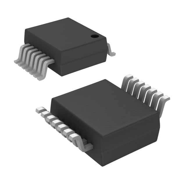
SN74LV166ADGVR is available in a small-sized TSSOP-16 package.
Essence
The essence of SN74LV166ADGVR lies in its ability to efficiently convert parallel data into serial data, making it suitable for various applications requiring data shifting and storage.
Packaging/Quantity
SN74LV166ADGVR is typically packaged in reels containing 2500 units.
Specifications
- Supply Voltage Range: 1.65V to 5.5V
- Data Transfer Rate: Up to 100 MHz
- Number of Input/Output Pins: 16
- Operating Temperature Range: -40°C to 85°C
- Logic Family: LV (Low Voltage)
- Package Type: TSSOP-16
Detailed Pin Configuration
The pin configuration of SN74LV166ADGVR is as follows:
┌───┬───┬───┬───┬───┬───┬───┬───┐
QH' | 1 | 2 | 3 | 4 | 5 | 6 | 7 | 8 |
QH  | 16| 15| 14| 13| 12| 11| 10| 9 |
   └───┴───┴───┴───┴───┴───┴───┴───┘
Functional Features
- Parallel-in/serial-out operation: Allows parallel data to be shifted out serially.
- Cascadable: Multiple devices can be connected in series for expanded functionality.
- Clear input: Provides the ability to reset the shift register to a known state.
- Clock input: Controls the shifting of data from the parallel inputs to the serial output.
Advantages and Disadvantages
Advantages
- Low-voltage operation enables compatibility with a wide range of systems.
- High-speed data transfer allows for efficient data processing.
- Schmitt-trigger inputs ensure reliable operation in noisy environments.
- Small package size saves board space in compact designs.
Disadvantages
- Limited number of input/output pins may restrict certain applications requiring more extensive connectivity options.
- Lack of built-in error detection or correction mechanisms may require additional circuitry for error handling.
Working Principles
SN74LV166ADGVR operates based on the principle of parallel-in/serial-out shifting. It accepts parallel data inputs and shifts them out serially, one bit at a time. The clock input controls the shifting process, synchronizing the movement of data through the shift register. The clear input allows resetting the register to a known initial state.
Detailed Application Field Plans
SN74LV166ADGVR finds applications in various fields where data shifting and storage are required. Some potential application areas include:
- Communication Systems: Used for data serialization and deserialization in communication protocols such as UART (Universal Asynchronous Receiver-Transmitter).
- Data Acquisition: Enables efficient conversion of parallel data from sensors or ADCs (Analog-to-Digital Converters) into serial format for further processing.
- Industrial Automation: Used in control systems for sequential logic implementation and data transfer between modules.
- Display Systems: Facilitates the conversion of parallel display data into a serial format for driving LED matrices or segment displays.
Detailed and Complete Alternative Models
Some alternative models that offer similar functionality to SN74LV166ADGVR are:
- CD4021B: A CMOS 8-stage parallel-in/serial-out shift register with similar voltage range and package options.
- 74HC595: A high-speed CMOS 8-bit serial-in/serial-out shift register with cascading capabilities.
- SN74HC165: A parallel-load 8-bit shift register with serial output, compatible with a wide voltage range.
These alternative models can be considered based on specific requirements and compatibility with existing designs.
Word count: 615 words
技術ソリューションにおける SN74LV166ADGVR の適用に関連する 10 件の一般的な質問と回答をリストします。
Sure! Here are 10 common questions and answers related to the application of SN74LV166ADGVR:
Q: What is SN74LV166ADGVR? A: SN74LV166ADGVR is a 8-bit parallel-in/serial-out shift register IC, commonly used in digital circuits.
Q: What is the operating voltage range for SN74LV166ADGVR? A: The operating voltage range for SN74LV166ADGVR is typically between 2V and 5.5V.
Q: How many inputs does SN74LV166ADGVR have? A: SN74LV166ADGVR has 8 parallel inputs (A-H) and 1 serial input (SER).
Q: What is the purpose of the serial output (QH') pin on SN74LV166ADGVR? A: The serial output (QH') pin provides the shifted data output from the last stage of the shift register.
Q: Can SN74LV166ADGVR be cascaded to increase the number of bits? A: Yes, multiple SN74LV166ADGVR ICs can be cascaded together to increase the number of bits in the shift register.
Q: What is the maximum clock frequency supported by SN74LV166ADGVR? A: SN74LV166ADGVR can support clock frequencies up to 100 MHz.
Q: Does SN74LV166ADGVR have any built-in latches or storage elements? A: No, SN74LV166ADGVR is a simple shift register without any built-in latches or storage elements.
Q: What is the typical power consumption of SN74LV166ADGVR? A: The typical power consumption of SN74LV166ADGVR is around 2.5mW.
Q: Can SN74LV166ADGVR be used in both synchronous and asynchronous applications? A: Yes, SN74LV166ADGVR can be used in both synchronous and asynchronous applications depending on the clock input.
Q: What are some common applications of SN74LV166ADGVR? A: SN74LV166ADGVR is commonly used in applications such as data storage, serial-to-parallel conversion, shift register applications, and digital communication systems.
Please note that these answers are general and may vary based on specific datasheet specifications and application requirements.