

SN74LV165ADGVR
Product Overview
Category
SN74LV165ADGVR belongs to the category of integrated circuits (ICs).
Use
It is commonly used as a parallel-in, serial-out shift register.
Characteristics
- Low-voltage operation
- High-speed data transfer
- Wide operating temperature range
- Small package size
- Low power consumption
Package
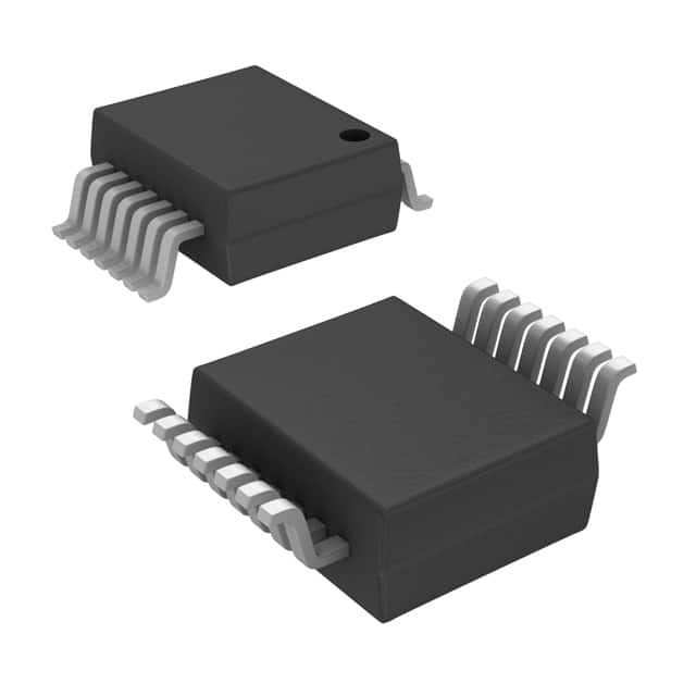
SN74LV165ADGVR is available in a small-sized VSSOP-16 package.
Essence
The essence of SN74LV165ADGVR lies in its ability to convert parallel data inputs into a serial output stream.
Packaging/Quantity
SN74LV165ADGVR is typically packaged in reels and comes in quantities of 2500 units per reel.
Specifications
- Supply Voltage: 2.7V to 5.5V
- Input Voltage Range: 0V to VCC
- Operating Temperature Range: -40°C to +85°C
- Output Current: ±6mA
- Clock Frequency: Up to 100MHz
Detailed Pin Configuration
- SER (Serial Data Input)
- QA (Parallel Data Output A)
- QB (Parallel Data Output B)
- QC (Parallel Data Output C)
- QD (Parallel Data Output D)
- QE (Parallel Data Output E)
- QF (Parallel Data Output F)
- QG (Parallel Data Output G)
- QH (Parallel Data Output H)
- CLK (Clock Input)
- SH/LD (Shift/Load Input)
- OE (Output Enable Input)
- GND (Ground)
- QH' (Serial Data Output)
- MR (Master Reset Input)
- VCC (Supply Voltage)
Functional Features
- Parallel-to-serial data conversion
- Shift and load functionality
- Output enable control
- Master reset capability
Advantages
- Low-voltage operation allows for compatibility with various systems
- High-speed data transfer enables efficient processing
- Wide operating temperature range ensures reliability in different environments
- Small package size saves board space
- Low power consumption contributes to energy efficiency
Disadvantages
- Limited number of parallel inputs (8 bits)
- Lack of built-in error detection or correction mechanisms
Working Principles
SN74LV165ADGVR operates by shifting the parallel data inputs into a serial output stream. The clock input controls the shifting process, while the shift/load input determines whether the data is shifted or loaded into the register. The output enable input enables or disables the parallel outputs. The master reset input resets the register to its initial state.
Detailed Application Field Plans
SN74LV165ADGVR finds applications in various fields, including: 1. Data communication systems 2. Industrial automation 3. Consumer electronics 4. Automotive electronics 5. Robotics
Detailed and Complete Alternative Models
Some alternative models that offer similar functionality to SN74LV165ADGVR are: 1. CD74HC165E 2. 74HC165D 3. MC74HC165AN 4. CD74HCT165E 5. 74HCT165D
These models can be considered as alternatives based on their specifications, pin configuration, and functional features.
Word count: 413 words
技術ソリューションにおける SN74LV165ADGVR の適用に関連する 10 件の一般的な質問と回答をリストします。
Sure! Here are 10 common questions and answers related to the application of SN74LV165ADGVR:
Question: What is the SN74LV165ADGVR?
- Answer: The SN74LV165ADGVR is a 8-bit parallel-in/serial-out shift register with a synchronous serial input and output.Question: What is the operating voltage range of SN74LV165ADGVR?
- Answer: The operating voltage range is from 2 V to 5.5 V.Question: What is the maximum clock frequency supported by SN74LV165ADGVR?
- Answer: The maximum clock frequency is 50 MHz.Question: Can I use multiple SN74LV165ADGVR devices in cascade?
- Answer: Yes, you can cascade multiple SN74LV165ADGVR devices to increase the number of inputs.Question: How many parallel inputs does SN74LV165ADGVR have?
- Answer: SN74LV165ADGVR has 8 parallel inputs.Question: Can I use SN74LV165ADGVR for both input and output operations?
- Answer: No, SN74LV165ADGVR is primarily used for input operations. For output operations, you may need a different device.Question: Does SN74LV165ADGVR have any built-in debounce circuitry?
- Answer: No, SN74LV165ADGVR does not have built-in debounce circuitry. You may need to implement external debounce circuitry if required.Question: What is the typical power consumption of SN74LV165ADGVR?
- Answer: The typical power consumption is around 2.5 mW.Question: Can I use SN74LV165ADGVR in both digital and analog circuits?
- Answer: SN74LV165ADGVR is primarily designed for digital circuits. It may not be suitable for analog applications.Question: Are there any application notes or reference designs available for SN74LV165ADGVR?
- Answer: Yes, you can refer to the datasheet of SN74LV165ADGVR for application notes and reference designs provided by the manufacturer.