

SN74LV04ADGVR
Product Overview
- Category: Integrated Circuit (IC)
- Use: Logic Gate
- Characteristics: Low-voltage, Hex Inverter
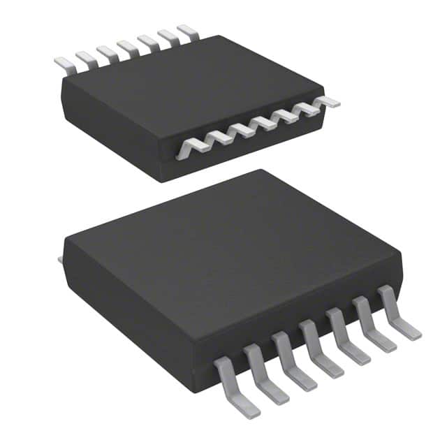
- Package: VSSOP (Very Small Outline Package)
- Essence: Inverting Logic Gate
- Packaging/Quantity: Tape and Reel, 2500 pieces per reel
Specifications
- Supply Voltage Range: 1.65V to 5.5V
- Input Voltage Range: 0V to VCC
- Output Voltage Range: 0V to VCC
- Maximum Operating Frequency: 50MHz
- Propagation Delay Time: 6ns (typical)
- Input Capacitance: 3.5pF (typical)
- Output Current: ±8mA
Detailed Pin Configuration
The SN74LV04ADGVR has a total of 14 pins arranged as follows:
__    __
   Y1 |1  \__/ 14| VCC
   A1 |2        13| Y6
   B1 |3        12| A6
   A2 |4   SN   11| B6
   B2 |5   74   10| A5
   Y2 |6   LV   9 | B5
  GND |7   04   8 | Y5
       ----------
Functional Features
- Hex Inverter: The SN74LV04ADGVR consists of six independent inverters, each capable of converting a logic level from high to low or vice versa.
- Low-Voltage Operation: It operates at a supply voltage range of 1.65V to 5.5V, making it suitable for low-power applications.
- High-Speed Performance: With a maximum operating frequency of 50MHz and a propagation delay time of 6ns, it provides fast and efficient logic operations.
- Wide Input Voltage Range: The input voltage can range from 0V to VCC, allowing compatibility with various logic families.
Advantages and Disadvantages
Advantages: - Low-voltage operation enables energy-efficient designs. - High-speed performance allows for quick signal processing. - Wide input voltage range ensures compatibility with different logic levels.
Disadvantages: - Limited output current may restrict its use in certain applications requiring higher current capabilities. - The small package size (VSSOP) may pose challenges during manual soldering or handling.
Working Principles
The SN74LV04ADGVR is based on complementary metal-oxide-semiconductor (CMOS) technology. Each inverter within the IC consists of a PMOS (p-channel metal-oxide-semiconductor) transistor and an NMOS (n-channel metal-oxide-semiconductor) transistor. When the input voltage is high, the PMOS transistor conducts, pulling the output voltage low. Conversely, when the input voltage is low, the NMOS transistor conducts, driving the output voltage high.
Detailed Application Field Plans
The SN74LV04ADGVR finds extensive use in various digital systems and electronic devices. Some application areas include:
- Microcontrollers and Microprocessors: It serves as a fundamental building block for logic operations in these devices.
- Communication Systems: It is utilized in signal processing, data transmission, and protocol conversion circuits.
- Consumer Electronics: The IC is employed in televisions, audio systems, and home appliances for signal conditioning and control functions.
- Automotive Electronics: It plays a crucial role in automotive control units, sensors, and infotainment systems.
- Industrial Automation: It is used in programmable logic controllers (PLCs), motor control circuits, and industrial instrumentation.
Detailed and Complete Alternative Models
- SN74LVC04A: Similar to SN74LV04ADGVR, but operates at a wider supply voltage range of 1.65V to 3.6V.
- SN74HCT04: A high-speed CMOS inverter with TTL (Transistor-Transistor Logic) compatibility.
- CD4069UB: A hex inverter IC with wide supply voltage range and high noise immunity.
These alternative models offer similar functionality and can be considered as replacements based on specific requirements.
In conclusion, the SN74LV04ADGVR is a low-voltage hex inverter IC that provides fast and efficient logic operations. Its small package size and wide input voltage range make it suitable for various digital systems and electronic devices. However, its limited output current and potential handling challenges should be taken into consideration during application design.
技術ソリューションにおける SN74LV04ADGVR の適用に関連する 10 件の一般的な質問と回答をリストします。
Sure! Here are 10 common questions and answers related to the application of SN74LV04ADGVR:
Q: What is SN74LV04ADGVR? A: SN74LV04ADGVR is a hex inverter gate IC, which means it has six independent inverters in a single package.
Q: What is the voltage supply range for SN74LV04ADGVR? A: The voltage supply range for SN74LV04ADGVR is typically between 2V and 5.5V.
Q: What is the maximum output current of SN74LV04ADGVR? A: The maximum output current of SN74LV04ADGVR is around 8mA.
Q: Can SN74LV04ADGVR be used in both digital and analog circuits? A: No, SN74LV04ADGVR is specifically designed for digital logic applications and is not suitable for analog circuits.
Q: What is the propagation delay of SN74LV04ADGVR? A: The propagation delay of SN74LV04ADGVR is typically around 6 ns.
Q: Can SN74LV04ADGVR handle high-speed signals? A: Yes, SN74LV04ADGVR is capable of handling high-speed signals due to its low propagation delay and fast switching characteristics.
Q: Is SN74LV04ADGVR compatible with TTL logic levels? A: Yes, SN74LV04ADGVR is compatible with TTL logic levels, making it suitable for interfacing with other TTL devices.
Q: Can SN74LV04ADGVR be used in battery-powered applications? A: Yes, SN74LV04ADGVR's low voltage supply range and low power consumption make it suitable for battery-powered applications.
Q: What is the package type of SN74LV04ADGVR? A: SN74LV04ADGVR comes in a small SOT-23 package, which is compact and suitable for space-constrained designs.
Q: Can SN74LV04ADGVR be used in automotive applications? A: Yes, SN74LV04ADGVR is qualified for automotive applications and can withstand the temperature and voltage requirements of such environments.
Please note that these answers are general and may vary depending on specific datasheet specifications and application requirements.