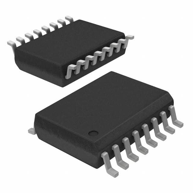
SN74HC594DW
Product Overview
Category
SN74HC594DW belongs to the category of integrated circuits (ICs).
Use
This product is commonly used in digital electronics and microcontroller-based systems for data storage, shift register functionality, and control signal generation.
Characteristics
- High-speed operation
- Wide operating voltage range
- Low power consumption
- Schmitt-trigger inputs for noise immunity
- Output current capability: 6 mA
- Output voltage: VCC - 0.5V
Package
SN74HC594DW is available in a standard SOIC (Small Outline Integrated Circuit) package.
Essence
The essence of SN74HC594DW lies in its ability to provide efficient data storage and serial-to-parallel conversion, making it an essential component in various digital applications.
Packaging/Quantity
SN74HC594DW is typically packaged in reels or tubes, with quantities varying based on customer requirements.
Specifications
- Supply voltage range: 2V to 6V
- Operating temperature range: -40°C to +85°C
- Input voltage range: 0V to VCC
- Maximum clock frequency: 25 MHz
- Number of output pins: 8
Detailed Pin Configuration
- GND (Ground)
- SER (Serial Data Input)
- SRCLK (Shift Register Clock Input)
- RCLK (Register Clock Input)
- OE (Output Enable)
- QH' (Serial Data Output)
- QA-QH (Parallel Data Outputs)
- VCC (Supply Voltage)
Functional Features
- Serial-in, parallel-out shift register
- Storage register with parallel outputs
- Cascadable for larger shift registers
- Output enable control for multiplexing applications
- Schmitt-trigger inputs for improved noise immunity
Advantages
- High-speed operation allows for efficient data transfer
- Wide operating voltage range provides flexibility in various applications
- Low power consumption contributes to energy-efficient designs
- Schmitt-trigger inputs ensure reliable performance in noisy environments
- Output current capability enables direct drive of external components
Disadvantages
- Limited number of output pins may restrict the complexity of certain applications
- Not suitable for high-voltage applications due to the maximum output voltage limitation
Working Principles
SN74HC594DW operates based on the principles of shift registers and parallel-to-serial conversion. It receives serial data through the SER pin, which is then shifted into the internal storage register using the SRCLK input. The RCLK input latches the stored data into the parallel output registers. The output enable (OE) pin controls the activation of the outputs.
Detailed Application Field Plans
SN74HC594DW finds extensive use in various applications, including but not limited to: 1. LED matrix displays 2. Multiplexed seven-segment displays 3. Serial data transmission systems 4. Data acquisition systems 5. Control signal generation in microcontroller-based projects
Detailed and Complete Alternative Models
Some alternative models that offer similar functionality to SN74HC594DW are: 1. CD74HC595E 2. 74HCT595 3. SN74LS595N 4. MC74HC595AN
These alternatives can be considered based on specific project requirements and availability.
In conclusion, SN74HC594DW is a versatile integrated circuit that provides efficient data storage, shift register functionality, and control signal generation. Its high-speed operation, wide voltage range, and low power consumption make it suitable for various digital applications. However, its limited number of output pins and voltage limitations should be taken into consideration when selecting this product for specific projects.
技術ソリューションにおける SN74HC594DW の適用に関連する 10 件の一般的な質問と回答をリストします。
Sure! Here are 10 common questions and answers related to the application of SN74HC594DW:
Q: What is SN74HC594DW? A: SN74HC594DW is a high-speed CMOS shift register with output storage registers. It can be used in various technical solutions for data shifting and control applications.
Q: What is the maximum operating voltage for SN74HC594DW? A: The maximum operating voltage for SN74HC594DW is 6 volts.
Q: How many output pins does SN74HC594DW have? A: SN74HC594DW has 8 output pins, labeled from Q0 to Q7.
Q: Can SN74HC594DW be cascaded to increase the number of outputs? A: Yes, SN74HC594DW can be cascaded by connecting the serial output (Q7) of one chip to the serial input (SER) of another chip, allowing for an increased number of outputs.
Q: What is the maximum clock frequency for SN74HC594DW? A: The maximum clock frequency for SN74HC594DW is typically around 100 MHz.
Q: Is SN74HC594DW compatible with both TTL and CMOS logic levels? A: Yes, SN74HC594DW is compatible with both TTL and CMOS logic levels, making it versatile for use in different systems.
Q: Can SN74HC594DW be used for driving LEDs or other low-power devices? A: Yes, SN74HC594DW can be used to drive LEDs or other low-power devices as it can sink up to 35mA per output pin.
Q: Does SN74HC594DW have any built-in protection features? A: SN74HC594DW has built-in diode clamps on the inputs to protect against electrostatic discharge (ESD) and other voltage spikes.
Q: Can SN74HC594DW be used in both parallel and serial data transfer modes? A: Yes, SN74HC594DW can be used in both parallel and serial data transfer modes, providing flexibility in different applications.
Q: What is the power supply voltage range for SN74HC594DW? A: The power supply voltage range for SN74HC594DW is typically between 2 volts and 6 volts.
Please note that these answers are general and may vary depending on the specific application and requirements.


