

SN74AUC32374ZKER
Product Overview
Category
The SN74AUC32374ZKER belongs to the category of integrated circuits (ICs).
Use
This IC is commonly used in digital systems for data storage and transfer.
Characteristics
- Low power consumption
- High-speed operation
- Wide operating voltage range
- Compatibility with various logic families
Package
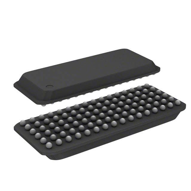
The SN74AUC32374ZKER is available in a small form factor package, such as a 48-pin TSSOP (Thin Shrink Small Outline Package).
Essence
The essence of this product lies in its ability to store and transfer digital data efficiently within electronic systems.
Packaging/Quantity
The SN74AUC32374ZKER is typically packaged in reels or tubes, with a quantity of 250 units per reel/tube.
Specifications
- Supply Voltage: 1.2V - 3.6V
- Operating Temperature Range: -40°C to +85°C
- Input/Output Type: Tri-State
- Number of Bits: 32
- Logic Family: AUC
Detailed Pin Configuration
The SN74AUC32374ZKER has a total of 48 pins, which are assigned specific functions. The pin configuration is as follows:
- Pin 1: Output Enable (OE)
- Pin 2: Data Input D0
- Pin 3: Data Input D1
- Pin 4: Data Input D2
- Pin 5: Data Input D3
- Pin 6: Data Input D4
- Pin 7: Data Input D5
- Pin 8: Data Input D6
- Pin 9: Data Input D7
- Pin 10: Data Input D8
- Pin 11: Data Input D9
- Pin 12: Data Input D10
- Pin 13: Data Input D11
- Pin 14: Data Input D12
- Pin 15: Data Input D13
- Pin 16: Data Input D14
- Pin 17: Data Input D15
- Pin 18: Output Q0
- Pin 19: Output Q1
- Pin 20: Output Q2
- Pin 21: Output Q3
- Pin 22: Output Q4
- Pin 23: Output Q5
- Pin 24: Output Q6
- Pin 25: Output Q7
- Pin 26: Output Q8
- Pin 27: Output Q9
- Pin 28: Output Q10
- Pin 29: Output Q11
- Pin 30: Output Q12
- Pin 31: Output Q13
- Pin 32: Output Q14
- Pin 33: Output Q15
- Pin 34: Output Enable (OE)
- Pin 35: Clock (CLK)
- Pin 36: Clock Enable (CE)
- Pin 37: Master Reset (MR)
- Pin 38: Data Input D16
- Pin 39: Data Input D17
- Pin 40: Data Input D18
- Pin 41: Data Input D19
- Pin 42: Data Input D20
- Pin 43: Data Input D21
- Pin 44: Data Input D22
- Pin 45: Data Input D23
- Pin 46: Data Input D24
- Pin 47: Data Input D25
- Pin 48: Data Input D26
Functional Features
- Tri-State Outputs: The SN74AUC32374ZKER features tri-state outputs, allowing for efficient data transfer and sharing between multiple devices.
- High-Speed Operation: This IC operates at high speeds, enabling rapid data processing and transmission.
- Low Power Consumption: With its low power consumption characteristics, the SN74AUC32374ZKER helps conserve energy in electronic systems.
- Wide Operating Voltage Range: The IC can operate within a wide voltage range, providing flexibility in various applications.
Advantages and Disadvantages
Advantages
- Efficient data storage and transfer capabilities
- Compatibility with different logic families
- Low power consumption
- High-speed operation
Disadvantages
- Limited number of bits (32)
- Requires careful handling due to small form factor package
Working Principles
The SN74AUC32374ZKER functions as a latch or flip-flop, storing digital data and allowing it to be transferred between different parts of a digital system. It operates based on clock signals and control inputs, which enable the storage and retrieval of data.
#
技術ソリューションにおける SN74AUC32374ZKER の適用に関連する 10 件の一般的な質問と回答をリストします。
Sure! Here are 10 common questions and answers related to the application of SN74AUC32374ZKER in technical solutions:
Q: What is SN74AUC32374ZKER? A: SN74AUC32374ZKER is a specific model of octal D-type flip-flop with 3-state outputs, manufactured by Texas Instruments.
Q: What is the purpose of SN74AUC32374ZKER? A: SN74AUC32374ZKER is used for storing and transferring digital data in various electronic systems.
Q: What is the operating voltage range of SN74AUC32374ZKER? A: The operating voltage range of SN74AUC32374ZKER is typically between 0.8V and 2.7V.
Q: How many flip-flops are there in SN74AUC32374ZKER? A: SN74AUC32374ZKER consists of 8 individual D-type flip-flops.
Q: What is the maximum clock frequency supported by SN74AUC32374ZKER? A: SN74AUC32374ZKER can operate at a maximum clock frequency of 200 MHz.
Q: Can SN74AUC32374ZKER be used in both synchronous and asynchronous applications? A: Yes, SN74AUC32374ZKER can be used in both synchronous and asynchronous applications.
Q: What is the output drive strength of SN74AUC32374ZKER? A: The output drive strength of SN74AUC32374ZKER is typically 12 mA.
Q: Does SN74AUC32374ZKER support 3-state outputs? A: Yes, SN74AUC32374ZKER supports 3-state outputs, allowing multiple devices to share a common bus.
Q: What is the package type of SN74AUC32374ZKER? A: SN74AUC32374ZKER is available in a 48-pin BGA (Ball Grid Array) package.
Q: Can SN74AUC32374ZKER be used in automotive applications? A: Yes, SN74AUC32374ZKER is qualified for automotive applications and meets the necessary standards.
Please note that these answers are general and may vary depending on the specific datasheet and application requirements.