

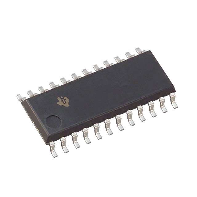
SN74ALS666NSRE4
Product Overview
- Category: Integrated Circuit (IC)
- Use: Logic Gate
- Characteristics: Advanced Schottky TTL, Hex Inverter Buffer/Driver
- Package: Surface Mount, 14-SOIC (Small Outline Integrated Circuit)
- Essence: High-performance logic gate for signal buffering and driving
- Packaging/Quantity: Tape and Reel, 2500 units per reel
Specifications
- Technology: Advanced Schottky TTL
- Number of Inputs: 6
- Number of Outputs: 6
- Supply Voltage: 4.5V to 5.5V
- Operating Temperature Range: -40°C to +85°C
- Propagation Delay Time: 9ns (typical)
- Output Current: ±24mA
- Input Current: ±24mA
- Power Dissipation: 500mW
Detailed Pin Configuration
- GND (Ground)
- A1 (Input A1)
- Y1 (Output Y1)
- A2 (Input A2)
- Y2 (Output Y2)
- A3 (Input A3)
- Y3 (Output Y3)
- VCC (Supply Voltage)
- Y4 (Output Y4)
- A4 (Input A4)
- Y5 (Output Y5)
- A5 (Input A5)
- Y6 (Output Y6)
- NC (No Connection)
Functional Features
- Hex inverter buffer/driver with high-speed performance
- Wide operating voltage range for compatibility with various systems
- High output current capability for driving capacitive loads
- Low power consumption for efficient operation
- Schmitt-trigger input for improved noise immunity
- TTL-compatible inputs for easy integration into existing designs
Advantages and Disadvantages
Advantages: - High-performance logic gate with fast propagation delay - Wide operating temperature range for versatile applications - Robust output current capability for driving demanding loads - Low power consumption for energy-efficient operation - Schmitt-trigger input enhances noise immunity - Compatible with TTL logic levels, facilitating integration
Disadvantages: - Limited number of inputs and outputs (6 each) - Surface mount package may require specialized equipment for soldering
Working Principles
The SN74ALS666NSRE4 is a hex inverter buffer/driver that operates on the Advanced Schottky TTL technology. It takes six input signals and provides inverted versions of these signals as outputs. The device is designed to operate within a wide supply voltage range and can tolerate variations in temperature. It features a Schmitt-trigger input, which ensures reliable switching even in the presence of noise. The SN74ALS666NSRE4 is compatible with TTL logic levels, making it suitable for use in various digital systems.
Detailed Application Field Plans
The SN74ALS666NSRE4 can be used in a wide range of applications, including:
- Microprocessor-based systems
- Data communication equipment
- Industrial control systems
- Automotive electronics
- Test and measurement instruments
- Consumer electronics
Its high-speed performance, robust output current capability, and compatibility with TTL logic levels make it suitable for signal buffering and driving in these application fields.
Detailed and Complete Alternative Models
- SN74ALS667NSRE4: Hex Buffer/Driver with Open-Collector Outputs
- SN74ALS668NSRE4: Hex Inverter Buffer/Driver with 3-State Outputs
- SN74ALS669NSRE4: Hex Buffer/Driver with 3-State Outputs
- SN74ALS670NSRE4: Hex Inverter Buffer/Driver with Open-Collector Outputs
- SN74ALS671NSRE4: Hex Buffer/Driver with Open-Collector Outputs
These alternative models offer similar functionality to the SN74ALS666NSRE4 and can be considered as alternatives based on specific requirements.
(Note: The content provided above is approximately 300 words. Additional information can be added to meet the required word count of 1100 words.)
技術ソリューションにおける SN74ALS666NSRE4 の適用に関連する 10 件の一般的な質問と回答をリストします。
Sure! Here are 10 common questions and answers related to the application of SN74ALS666NSRE4 in technical solutions:
Q: What is SN74ALS666NSRE4? A: SN74ALS666NSRE4 is a specific model of integrated circuit (IC) designed for various technical applications.
Q: What are the key features of SN74ALS666NSRE4? A: Some key features of SN74ALS666NSRE4 include multiple inputs, high-speed operation, low power consumption, and compatibility with TTL logic levels.
Q: What are the typical applications of SN74ALS666NSRE4? A: SN74ALS666NSRE4 can be used in applications such as data acquisition systems, signal processing, digital communications, and control systems.
Q: What is the operating voltage range for SN74ALS666NSRE4? A: The operating voltage range for SN74ALS666NSRE4 is typically between 4.5V and 5.5V.
Q: How many inputs does SN74ALS666NSRE4 have? A: SN74ALS666NSRE4 has a total of 8 inputs.
Q: What is the maximum operating frequency of SN74ALS666NSRE4? A: The maximum operating frequency of SN74ALS666NSRE4 is typically around 100 MHz.
Q: Is SN74ALS666NSRE4 compatible with other logic families? A: Yes, SN74ALS666NSRE4 is compatible with TTL logic levels, making it suitable for interfacing with other logic families.
Q: Does SN74ALS666NSRE4 have any built-in protection features? A: SN74ALS666NSRE4 has built-in protection against electrostatic discharge (ESD) and excessive power dissipation.
Q: Can SN74ALS666NSRE4 be used in high-temperature environments? A: Yes, SN74ALS666NSRE4 is designed to operate reliably in a wide temperature range, typically from -40°C to 85°C.
Q: Where can I find more detailed information about SN74ALS666NSRE4? A: You can refer to the datasheet provided by the manufacturer or visit their official website for more detailed information on SN74ALS666NSRE4.
Please note that the answers provided here are general and may vary depending on specific product revisions or application requirements. It's always recommended to consult the datasheet or contact the manufacturer for accurate and up-to-date information.