

SN74AHC125RGYR
Product Overview
- Category: Integrated Circuit (IC)
- Use: Buffer/Driver
- Characteristics: High-speed, low-power, non-inverting
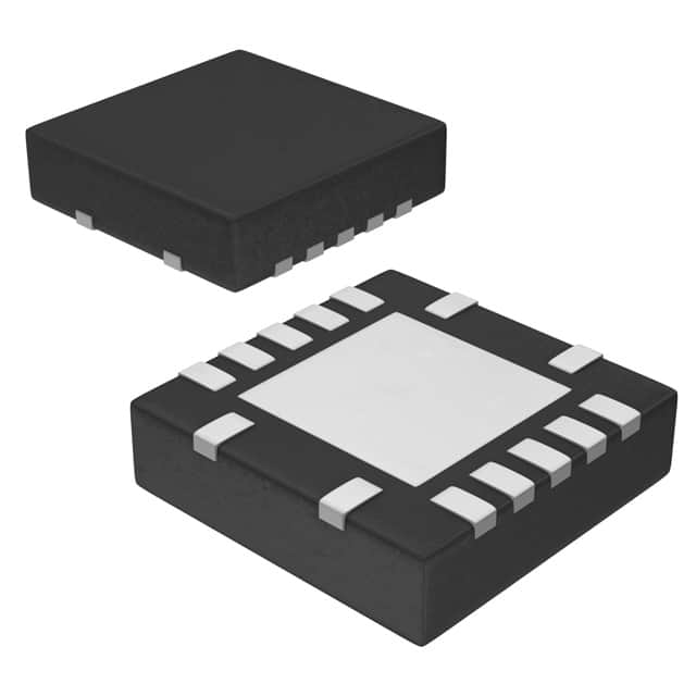
- Package: 14-pin VQFN (Very Thin Quad Flat No-Lead) package
- Essence: Logic level translator/buffer
- Packaging/Quantity: Tape and reel packaging, 2500 units per reel
Specifications
- Supply Voltage Range: 2 V to 5.5 V
- Input Voltage Range: 0 V to VCC
- Output Voltage Range: 0 V to VCC
- Maximum Operating Frequency: 50 MHz
- Number of Channels: 4
- Input Capacitance: 3 pF
- Output Capacitance: 6 pF
- Propagation Delay Time: 7 ns
- Operating Temperature Range: -40°C to +85°C
Detailed Pin Configuration
The SN74AHC125RGYR has a total of 14 pins, which are labeled as follows:
- OE (Output Enable) 1
- Y1 (Output) 1
- A1 (Input) 1
- GND (Ground)
- A2 (Input) 2
- Y2 (Output) 2
- OE (Output Enable) 2
- VCC (Supply Voltage)
- Y3 (Output) 3
- A3 (Input) 3
- GND (Ground)
- A4 (Input) 4
- Y4 (Output) 4
- OE (Output Enable) 4
Functional Features
- Non-inverting buffer/driver with 3-state outputs
- Allows voltage level translation between different logic families
- High-speed operation with low power consumption
- Supports bidirectional data flow
- Output enable (OE) pin allows for easy control of output state
Advantages and Disadvantages
Advantages: - High-speed operation enables efficient data transfer - Low-power design helps conserve energy - Non-inverting nature simplifies logic level translation - 3-state outputs provide flexibility in controlling signal flow
Disadvantages: - Limited number of channels (4) - Propagation delay time may impact timing-sensitive applications - Requires careful consideration of voltage compatibility with connected devices
Working Principles
The SN74AHC125RGYR is a buffer/driver IC that operates as a non-inverting logic level translator. It takes input signals from one logic family and provides output signals compatible with another logic family. The device uses CMOS technology, allowing for high-speed operation while consuming minimal power.
The OE pins control the output state of the device. When the OE pin is low, the outputs are enabled and mirror the inputs. Conversely, when the OE pin is high, the outputs are in a high-impedance state, effectively disconnecting them from the circuit.
The SN74AHC125RGYR can be used to interface between different logic families, such as TTL (Transistor-Transistor Logic) and CMOS (Complementary Metal-Oxide-Semiconductor). It ensures proper voltage level translation and signal integrity between these incompatible systems.
Detailed Application Field Plans
The SN74AHC125RGYR finds applications in various fields, including:
- Microcontroller interfacing: It facilitates communication between microcontrollers operating at different logic levels.
- Data transmission: It enables voltage level translation in serial communication interfaces like UART, SPI, and I2C.
- Industrial automation: The IC is used in control systems to interface between different logic families.
- Automotive electronics: It plays a vital role in connecting various components with different voltage requirements.
- Consumer electronics: The IC is utilized in devices that require logic level translation, such as smartphones and tablets.
Detailed and Complete Alternative Models
- SN74AHC125PW: 14-pin TSSOP (Thin Shrink Small Outline Package) package
- SN74AHC125NSR: 14-pin SOIC (Small Outline Integrated Circuit) package
- SN74AHC125D: 14-pin SOIC package with wider temperature range (-40°C to +125°C)
- SN74AHC125PWR: 14-pin TSSOP package with tape and reel packaging
These alternative models offer similar functionality and characteristics to the SN74AHC125RGYR, providing options for different package types and temperature ranges.
Word count: 487 words
技術ソリューションにおける SN74AHC125RGYR の適用に関連する 10 件の一般的な質問と回答をリストします。
Sure! Here are 10 common questions and answers related to the application of SN74AHC125RGYR in technical solutions:
Q: What is the SN74AHC125RGYR? A: The SN74AHC125RGYR is a quad bus buffer gate with 3-state outputs, commonly used for signal buffering and level shifting in digital circuits.
Q: What is the operating voltage range of SN74AHC125RGYR? A: The operating voltage range of SN74AHC125RGYR is typically between 2V and 5.5V.
Q: How many channels does SN74AHC125RGYR have? A: SN74AHC125RGYR has four independent channels, each with a separate input and output.
Q: What is the maximum output current of SN74AHC125RGYR? A: The maximum output current per channel of SN74AHC125RGYR is typically 8mA.
Q: Can SN74AHC125RGYR be used for level shifting between different voltage domains? A: Yes, SN74AHC125RGYR can be used for level shifting as it supports voltage translation between different logic levels.
Q: What is the propagation delay of SN74AHC125RGYR? A: The typical propagation delay of SN74AHC125RGYR is around 5ns.
Q: Is SN74AHC125RGYR compatible with both CMOS and TTL logic levels? A: Yes, SN74AHC125RGYR is compatible with both CMOS (3.3V) and TTL (5V) logic levels.
Q: Can SN74AHC125RGYR be used for bidirectional data transfer? A: No, SN74AHC125RGYR is a unidirectional buffer and does not support bidirectional data transfer.
Q: What is the package type of SN74AHC125RGYR? A: SN74AHC125RGYR is available in a small-outline integrated circuit (SOIC) package.
Q: Can SN74AHC125RGYR handle high-speed signals? A: Yes, SN74AHC125RGYR is designed to handle high-speed signals and can be used in applications with fast switching speeds.
Please note that the answers provided here are general and may vary depending on specific datasheet specifications and application requirements.