

MSC1213Y5PAGR
Product Overview
Category: Integrated Circuit (IC)
Use: The MSC1213Y5PAGR is a high-performance analog-to-digital converter (ADC) designed for precision measurement applications. It offers accurate conversion of analog signals into digital data, making it suitable for various industrial and scientific purposes.
Characteristics: - High resolution: The MSC1213Y5PAGR provides a resolution of up to 24 bits, ensuring precise measurement accuracy. - Low power consumption: This ADC operates at low power levels, making it energy-efficient and suitable for battery-powered devices. - Wide input voltage range: It can handle a wide range of input voltages, allowing for versatile usage in different scenarios. - Fast conversion speed: The MSC1213Y5PAGR offers fast conversion times, enabling real-time data acquisition.
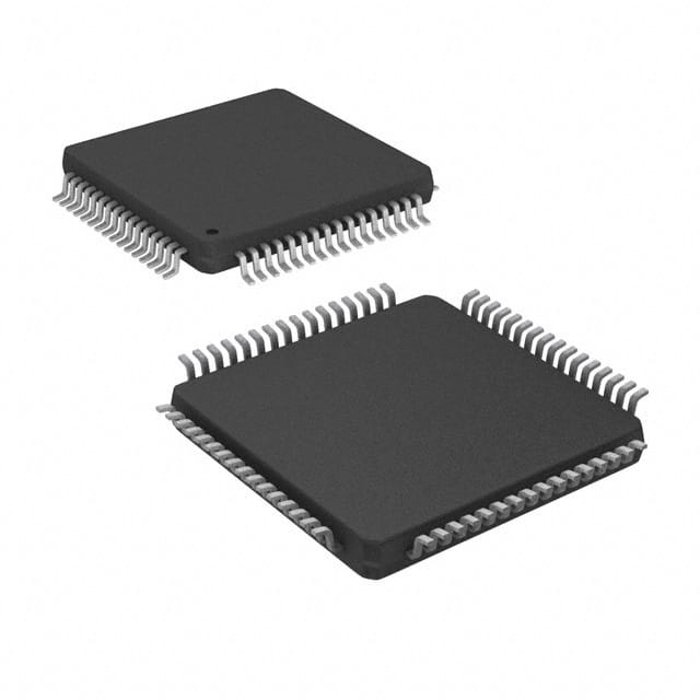
Package: The MSC1213Y5PAGR comes in a small form factor package, making it suitable for space-constrained applications. It is available in a surface-mount package, which facilitates easy integration onto circuit boards.
Essence: The essence of the MSC1213Y5PAGR lies in its ability to accurately convert analog signals into digital data, providing precise measurements for various applications.
Packaging/Quantity: The MSC1213Y5PAGR is typically sold in reels or tubes, with a quantity of 250 units per reel/tube.
Specifications
- Resolution: Up to 24 bits
- Input Voltage Range: ±10V
- Conversion Speed: 100 kSPS (Samples Per Second)
- Power Supply: 2.7V to 5.25V
- Operating Temperature Range: -40°C to +85°C
- Package Type: VQFN-32
Detailed Pin Configuration
The MSC1213Y5PAGR has a total of 32 pins, which are assigned specific functions. The pin configuration is as follows:
- VREFP: Positive reference voltage input
- VREFN: Negative reference voltage input
- AGND: Analog ground
- AVDD: Analog power supply
- DVDD: Digital power supply
- DGND: Digital ground
- CLK: Clock input
- CS: Chip select input
- DIN: Serial data input
- DOUT: Serial data output
- SCLK: Serial clock input
- SDI: Serial data input
- SDO: Serial data output
- SDO/TRI-STATE: Serial data output or tri-state control
- SDO/SDI: Serial data output or serial data input
- SDO/SCLK: Serial data output or serial clock input
- SDO/CS: Serial data output or chip select input
- REFOUT: Reference voltage output
- REFBUF: Reference buffer output
- REFBUFEN: Reference buffer enable
- REFBUFIN: Reference buffer input
- REFBUFINEN: Reference buffer input enable
- REFBUFINTRI: Reference buffer input tri-state control
- REFBUFINTRIEN: Reference buffer input tri-state control enable
- REFBUFINTRIENB: Reference buffer input tri-state control enable (inverted)
- REFBUFINTRIENB: Reference buffer input tri-state control enable (inverted)
- REFBUFINTRIENB: Reference buffer input tri-state control enable (inverted)
- REFBUFINTRIENB: Reference buffer input tri-state control enable (inverted)
- REFBUFINTRIENB: Reference buffer input tri-state control enable (inverted)
- REFBUFINTRIENB: Reference buffer input tri-state control enable (inverted)
- REFBUFINTRIENB: Reference buffer input tri-state control enable (inverted)
- REFBUFINTRIENB: Reference buffer input tri-state control enable (inverted)
Functional Features
- High-resolution conversion: The MSC1213Y5PAGR offers up to 24-bit resolution, ensuring accurate measurement of analog signals.
- Low power consumption: It operates at low power levels, making it suitable for battery-powered devices and energy-efficient applications.
- Flexible input voltage range: The ADC can handle a wide range of input voltages, allowing for versatile usage in different scenarios.
- Fast conversion speed: With a conversion speed of 100 kSPS, the MSC1213Y5PAGR enables real-time data acquisition.
- Serial interface: It features a serial interface for easy integration with microcontrollers and other digital systems.
Advantages and Disadvantages
Advantages: - High resolution ensures precise measurements - Low power consumption for energy efficiency - Wide input voltage range allows for versatile usage
技術ソリューションにおける MSC1213Y5PAGR の適用に関連する 10 件の一般的な質問と回答をリストします。
What is the operating voltage range of MSC1213Y5PAGR?
- The operating voltage range of MSC1213Y5PAGR is 2.7V to 5.25V.Can MSC1213Y5PAGR be used for temperature sensing applications?
- Yes, MSC1213Y5PAGR can be used for temperature sensing applications.What is the resolution of the ADC in MSC1213Y5PAGR?
- The ADC in MSC1213Y5PAGR has a resolution of 12 bits.Is MSC1213Y5PAGR suitable for battery-powered devices?
- Yes, MSC1213Y5PAGR is suitable for battery-powered devices due to its low power consumption.Can MSC1213Y5PAGR be interfaced with microcontrollers?
- Yes, MSC1213Y5PAGR can be easily interfaced with microcontrollers using standard communication protocols.What is the typical conversion time of MSC1213Y5PAGR?
- The typical conversion time of MSC1213Y5PAGR is 1.1ms.Does MSC1213Y5PAGR have built-in programmable gain amplifiers (PGAs)?
- Yes, MSC1213Y5PAGR features built-in PGAs for signal conditioning.Can MSC1213Y5PAGR be used in industrial automation systems?
- Yes, MSC1213Y5PAGR is suitable for use in industrial automation systems.What is the temperature range for proper operation of MSC1213Y5PAGR?
- MSC1213Y5PAGR is designed to operate within a temperature range of -40°C to 125°C.Is MSC1213Y5PAGR RoHS compliant?
- Yes, MSC1213Y5PAGR is RoHS compliant, making it suitable for environmentally conscious designs.