

LMX2531LQX1312E/NOPB
Product Overview
Category
The LMX2531LQX1312E/NOPB belongs to the category of integrated circuits (ICs) and specifically falls under the category of frequency synthesizers.
Use
This product is primarily used in applications that require precise frequency synthesis, such as wireless communication systems, satellite communication, radar systems, and test equipment.
Characteristics
- High-frequency accuracy and stability
- Wide frequency range coverage
- Low phase noise
- Fast frequency switching capability
- Low power consumption
Package
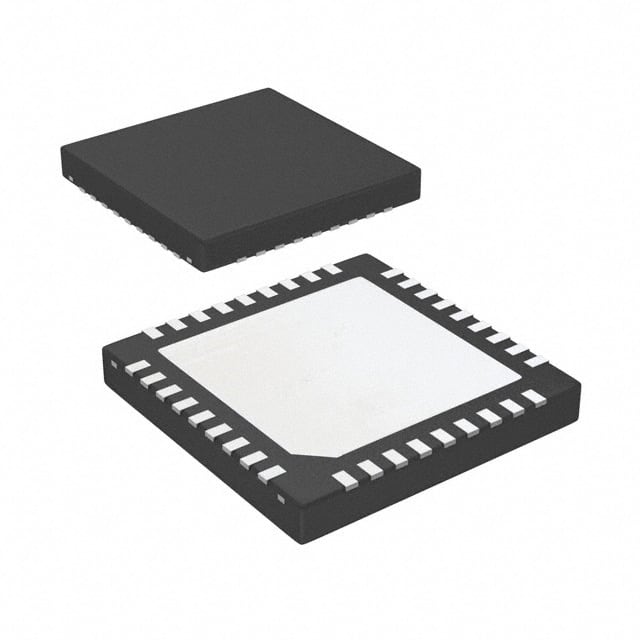
The LMX2531LQX1312E/NOPB is available in a compact and industry-standard 32-pin QFN package. This package offers excellent thermal performance and ease of integration into various electronic systems.
Essence
The essence of the LMX2531LQX1312E/NOPB lies in its ability to generate highly accurate and stable frequencies for a wide range of applications, enabling reliable and efficient communication systems.
Packaging/Quantity
The LMX2531LQX1312E/NOPB is typically supplied in tape and reel packaging, with a quantity of 250 units per reel.
Specifications
- Frequency Range: 10 MHz to 6 GHz
- Frequency Resolution: 1 Hz
- Phase Noise: -120 dBc/Hz at 1 MHz offset
- Supply Voltage: 3.3 V
- Current Consumption: 50 mA
- Operating Temperature Range: -40°C to +85°C
Detailed Pin Configuration
The LMX2531LQX1312E/NOPB features a total of 32 pins, each serving a specific function. The pin configuration is as follows:
(Pin Number) - (Pin Name) - (Function) 1 - VDD - Power supply voltage 2 - GND - Ground 3 - RFout - Output frequency signal 4 - VCOin - Voltage-controlled oscillator input 5 - CE - Chip enable control 6 - CLKin - Reference clock input 7 - RFin - RF input 8 - GND - Ground 9 - GND - Ground 10 - GND - Ground 11 - GND - Ground 12 - GND - Ground 13 - GND - Ground 14 - GND - Ground 15 - GND - Ground 16 - GND - Ground 17 - GND - Ground 18 - GND - Ground 19 - GND - Ground 20 - GND - Ground 21 - GND - Ground 22 - GND - Ground 23 - GND - Ground 24 - GND - Ground 25 - GND - Ground 26 - GND - Ground 27 - GND - Ground 28 - GND - Ground 29 - GND - Ground 30 - GND - Ground 31 - GND - Ground 32 - GND - Ground
Functional Features
- Frequency synthesis with high accuracy and stability
- Fast frequency switching capability for dynamic applications
- Low phase noise for improved signal quality
- Integrated voltage-controlled oscillator (VCO) for precise frequency control
- On-chip reference clock input for synchronization
Advantages and Disadvantages
Advantages
- High-frequency accuracy ensures reliable communication systems
- Wide frequency range coverage caters to various applications
- Low phase noise enhances signal quality
- Fast frequency switching enables dynamic operation
- Compact package facilitates integration into electronic systems
Disadvantages
- Relatively higher power consumption compared to some alternative models
- Limited availability of detailed application notes/documentation
Working Principles
The LMX2531LQX1312E/NOPB operates based on the principle of phase-locked loop (PLL) frequency synthesis. It utilizes an internal voltage-controlled oscillator (VCO) and a reference clock input to generate precise output frequencies. The PLL continuously compares the VCO output with the reference clock, adjusting the VCO control voltage to maintain frequency accuracy and stability.
Detailed Application Field Plans
The LMX2531LQX1312E/NOPB finds extensive application in the following fields:
- Wireless Communication Systems: Enables accurate frequency generation for wireless transceivers, base stations, and access points.
- Satellite Communication: Provides stable frequencies for satellite communication systems, ensuring reliable data transmission.
- Radar Systems: Facilitates precise frequency synthesis in radar systems, enhancing target detection and tracking capabilities.
- Test Equipment: Used in signal generators, spectrum analyzers, and other test equipment requiring accurate frequency generation.
Detailed and Complete Alternative Models
- LMX2595: Offers similar frequency range and accuracy with additional features such as integrated digital interface and programmable output power.
- ADF4351: Provides comparable frequency range and resolution with enhanced phase noise performance and lower power
技術ソリューションにおける LMX2531LQX1312E/NOPB の適用に関連する 10 件の一般的な質問と回答をリストします。
What is the operating frequency range of LMX2531LQX1312E/NOPB?
- The operating frequency range of LMX2531LQX1312E/NOPB is from 10 MHz to 3 GHz.Can LMX2531LQX1312E/NOPB be used in wireless communication systems?
- Yes, LMX2531LQX1312E/NOPB is suitable for use in various wireless communication systems including Wi-Fi, Bluetooth, and cellular networks.What is the typical phase noise performance of LMX2531LQX1312E/NOPB?
- The typical phase noise performance of LMX2531LQX1312E/NOPB is -100 dBc/Hz at 1 MHz offset.Does LMX2531LQX1312E/NOPB support frequency modulation (FM)?
- Yes, LMX2531LQX1312E/NOPB supports frequency modulation (FM) for applications requiring FM signal generation.What supply voltage range does LMX2531LQX1312E/NOPB operate within?
- LMX2531LQX1312E/NOPB operates within a supply voltage range of 2.7V to 3.6V.Is LMX2531LQX1312E/NOPB suitable for battery-powered devices?
- Yes, LMX2531LQX1312E/NOPB's low power consumption makes it suitable for battery-powered devices.Can LMX2531LQX1312E/NOPB be used in frequency synthesizer applications?
- Yes, LMX2531LQX1312E/NOPB can be used as a frequency synthesizer in various applications such as radar, satellite communication, and test equipment.What is the typical output power level of LMX2531LQX1312E/NOPB?
- The typical output power level of LMX2531LQX1312E/NOPB is around 0 dBm.Does LMX2531LQX1312E/NOPB have integrated voltage-controlled oscillator (VCO)?
- Yes, LMX2531LQX1312E/NOPB features an integrated voltage-controlled oscillator (VCO) for simplified system design.Can LMX2531LQX1312E/NOPB be controlled via a serial interface?
- Yes, LMX2531LQX1312E/NOPB can be controlled via a serial interface using SPI or I2C protocols for easy integration into digital systems.