

DS90CR485VS/NOPB
Product Overview
- Category: Integrated Circuit (IC)
- Use: High-speed differential line driver and receiver
- Characteristics:
- Supports data rates up to 155 Mbps
- Operates with a single 3.3V power supply
- Compatible with LVDS, LVPECL, CML, and HSTL logic levels
- Low power consumption
- Small package size
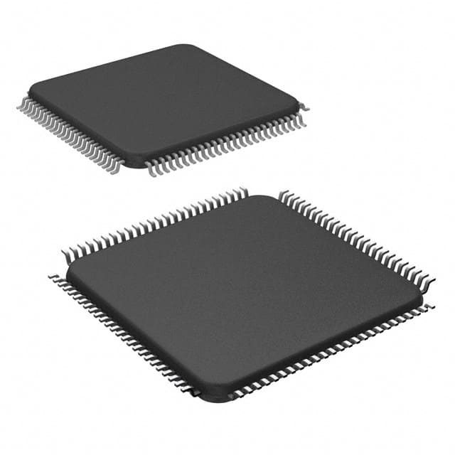
- Package: SOP-8 (Small Outline Package)
- Essence: The DS90CR485VS/NOPB is a high-performance differential line driver and receiver designed for high-speed data transmission applications.
- Packaging/Quantity: Available in tape and reel packaging, with 2500 units per reel.
Specifications
- Data Rate: Up to 155 Mbps
- Supply Voltage: 3.3V ±10%
- Operating Temperature Range: -40°C to +85°C
- Input Common Mode Voltage Range: -2V to +2V
- Output Voltage Swing: 350mV (minimum) differential
- Propagation Delay: 1.5ns (typical)
- Power Consumption: 100mW (typical)
Pin Configuration
The DS90CR485VS/NOPB features an SOP-8 package with the following pin configuration:
Pin 1: VCC
   Pin 2: GND
   Pin 3: RIN-
   Pin 4: RIN+
   Pin 5: ROUT+
   Pin 6: ROUT-
   Pin 7: VIN-
   Pin 8: VIN+
Functional Features
- High-speed differential signaling for reliable data transmission.
- Wide input common mode voltage range allows compatibility with various logic levels.
- Low power consumption makes it suitable for power-sensitive applications.
- Small package size enables space-efficient designs.
Advantages and Disadvantages
Advantages: - Supports high data rates up to 155 Mbps. - Compatible with multiple logic levels. - Low power consumption. - Compact package size.
Disadvantages: - Limited operating temperature range (-40°C to +85°C). - Requires a 3.3V power supply.
Working Principles
The DS90CR485VS/NOPB utilizes differential signaling to transmit data at high speeds. It receives differential input signals and converts them into single-ended outputs. The device operates with a single 3.3V power supply and is compatible with various logic levels, including LVDS, LVPECL, CML, and HSTL.
Application Field Plans
The DS90CR485VS/NOPB is commonly used in the following application fields:
- High-speed data communication systems
- Video transmission and display systems
- Industrial automation and control systems
- Medical imaging equipment
- Test and measurement instruments
Alternative Models
Below are some alternative models that offer similar functionality:
- SN65LVDS31 (Texas Instruments)
- MAX9126 (Maxim Integrated)
- DS90CR287 (Texas Instruments)
- MC100EP16 (ON Semiconductor)
These alternative models can be considered based on specific requirements and design considerations.
Word count: 314 words
技術ソリューションにおける DS90CR485VS/NOPB の適用に関連する 10 件の一般的な質問と回答をリストします。
What is the DS90CR485VS/NOPB?
- The DS90CR485VS/NOPB is a 28-bit channel link serializer/deserializer (SerDes) designed for high-speed point-to-point data transmission.
What is the maximum data rate supported by DS90CR485VS/NOPB?
- The DS90CR485VS/NOPB supports a maximum data rate of 1.6 Gbps per channel.
What are the typical applications of DS90CR485VS/NOPB?
- Typical applications include flat panel displays, digital signage, and other multimedia systems requiring high-speed data transmission.
Does DS90CR485VS/NOPB support HDCP encryption?
- No, the DS90CR485VS/NOPB does not support HDCP encryption.
What is the power supply voltage range for DS90CR485VS/NOPB?
- The power supply voltage range is typically between 3.0V and 3.6V.
Is DS90CR485VS/NOPB compatible with LVDS standards?
- Yes, the DS90CR485VS/NOPB is compatible with Low Voltage Differential Signaling (LVDS) standards.
Can DS90CR485VS/NOPB be used in automotive applications?
- Yes, DS90CR485VS/NOPB can be used in automotive applications, provided it meets the necessary environmental and safety requirements.
What is the operating temperature range for DS90CR485VS/NOPB?
- The operating temperature range is typically between -40°C to 85°C.
Does DS90CR485VS/NOPB support daisy-chaining multiple devices?
- Yes, DS90CR485VS/NOPB supports daisy-chaining for extending the number of channels.
Are evaluation modules available for DS90CR485VS/NOPB?
- Yes, evaluation modules are available to facilitate testing and development with DS90CR485VS/NOPB.