

DAC7563TDGSR
Product Overview
Category: Digital-to-Analog Converter (DAC)
Use: The DAC7563TDGSR is a high-performance, low-power, 12-bit digital-to-analog converter. It is designed to convert digital signals into analog voltages with high precision and accuracy.
Characteristics: - High resolution: 12-bit resolution allows for fine-grained control of the output voltage. - Low power consumption: The DAC7563TDGSR operates at low power levels, making it suitable for battery-powered applications. - Small package size: The device comes in a small TSSOP-16 package, which makes it ideal for space-constrained designs. - Wide operating temperature range: The DAC7563TDGSR can operate in temperatures ranging from -40°C to +125°C, making it suitable for harsh environments.
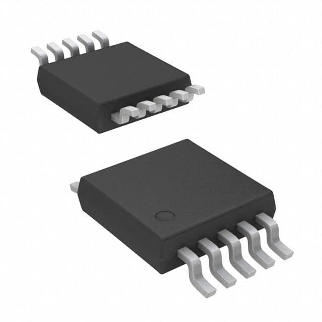
Package and Quantity: The DAC7563TDGSR is available in a TSSOP-16 package. Each package contains one DAC7563TDGSR device.
Specifications
- Resolution: 12 bits
- Number of Channels: 2
- Output Type: Voltage
- Interface: Serial (SPI)
- Supply Voltage: 2.7V to 5.5V
- Output Voltage Range: 0V to Vref
- Operating Temperature Range: -40°C to +125°C
- Power Consumption: 0.6mW (typical)
Pin Configuration
The DAC7563TDGSR has a total of 16 pins, arranged as follows:
┌───┬───┬───┬───┐
   │ 1 │ 2 │ 3 │ 4 │
   ├───┼───┼───┼───┤
   │ 5 │ 6 │ 7 │ 8 │
   ├───┼───┼───┼───┤
   │ 9 │10 │11 │12 │
   ├───┼───┼───┼───┤
   │13 │14 │15 │16 │
   └───┴───┴───┴───┘
- Pin 1: VrefB (Reference Voltage B)
- Pin 2: VoutB (Output Voltage B)
- Pin 3: AGND (Analog Ground)
- Pin 4: VDD (Power Supply)
- Pin 5: VrefA (Reference Voltage A)
- Pin 6: VoutA (Output Voltage A)
- Pin 7: DGND (Digital Ground)
- Pin 8: SCLK (Serial Clock Input)
- Pin 9: DIN (Data Input)
- Pin 10: SYNC (Chip Select)
- Pin 11: LDAC (Load DAC Register)
- Pin 12: CLR (Clear DAC Register)
- Pin 13: A0 (Address Bit 0)
- Pin 14: A1 (Address Bit 1)
- Pin 15: A2 (Address Bit 2)
- Pin 16: REFOUT (Reference Output)
Functional Features
- Dual-channel operation: The DAC7563TDGSR has two independent channels, allowing for simultaneous conversion of two digital signals into analog voltages.
- Serial interface: The device uses a serial peripheral interface (SPI) for communication with a microcontroller or other digital devices.
- Power-on reset: The DAC7563TDGSR includes a power-on reset circuit that ensures the outputs are set to zero volts upon power-up.
- Internal reference: The device features an internal voltage reference, eliminating the need for an external reference voltage source.
Advantages and Disadvantages
Advantages: - High resolution allows for precise control of analog output. - Low power consumption makes it suitable for battery-powered applications. - Small package size saves board space. - Wide operating temperature range enables use in harsh environments.
Disadvantages: - Limited number of channels (2) may not be sufficient for certain applications requiring more outputs. - Serial interface may require additional hardware or software implementation.
Working Principles
The DAC7563TDGSR works by converting digital input data into corresponding analog voltages. The digital data is received through the serial interface and stored in internal registers. The device then converts the digital values into analog voltages using a digital-to-analog conversion process. The converted analog voltages are available at the output pins, which can be connected to external circuitry for further processing or utilization.
Detailed Application Field Plans
The DAC7563TDGSR is widely used in various applications that require accurate and precise analog voltage generation. Some common application fields include:
- Industrial Automation: The DAC7563TDGSR can
技術ソリューションにおける DAC7563TDGSR の適用に関連する 10 件の一般的な質問と回答をリストします。
Sure! Here are 10 common questions and answers related to the application of DAC7563TDGSR:
Q: What is DAC7563TDGSR? A: DAC7563TDGSR is a digital-to-analog converter (DAC) integrated circuit that converts digital signals into analog voltage or current outputs.
Q: What is the operating voltage range of DAC7563TDGSR? A: The operating voltage range of DAC7563TDGSR is typically between 2.7V and 5.5V.
Q: How many channels does DAC7563TDGSR have? A: DAC7563TDGSR has two independent channels, allowing for simultaneous conversion of two different digital inputs.
Q: What is the resolution of DAC7563TDGSR? A: DAC7563TDGSR has a resolution of 12 bits, which means it can provide 4096 discrete output levels.
Q: Can DAC7563TDGSR be used for both voltage and current output applications? A: Yes, DAC7563TDGSR can be configured to provide either voltage or current outputs, depending on the application requirements.
Q: What is the maximum output voltage range of DAC7563TDGSR? A: The maximum output voltage range of DAC7563TDGSR is typically between 0V and Vref, where Vref is the reference voltage supplied to the IC.
Q: Does DAC7563TDGSR support SPI interface? A: Yes, DAC7563TDGSR supports Serial Peripheral Interface (SPI) communication protocol, making it easy to interface with microcontrollers or other digital devices.
Q: What is the settling time of DAC7563TDGSR? A: The settling time of DAC7563TDGSR is typically around 10 microseconds, ensuring fast and accurate conversion of digital signals to analog outputs.
Q: Can DAC7563TDGSR operate in both single-ended and differential modes? A: Yes, DAC7563TDGSR can be configured to operate in either single-ended or differential mode, providing flexibility in different applications.
Q: What are some typical applications of DAC7563TDGSR? A: DAC7563TDGSR is commonly used in various technical solutions such as industrial automation, process control, motor control, audio equipment, and instrumentation, where precise analog voltage or current outputs are required.
Please note that the answers provided here are general and may vary depending on specific datasheet specifications and application requirements.