

CDCVF111FNRG4
Overview
Category
CDCVF111FNRG4 belongs to the category of integrated circuits (ICs).
Use
This product is commonly used in electronic devices for signal conditioning and clock distribution.
Characteristics
- Signal conditioning: CDCVF111FNRG4 is designed to condition and shape digital signals, ensuring reliable transmission.
- Clock distribution: It provides multiple outputs for distributing clock signals to various components within a system.
- High-speed operation: This IC operates at high frequencies, making it suitable for applications requiring fast data processing.
- Low power consumption: CDCVF111FNRG4 is designed to minimize power consumption, enhancing energy efficiency in electronic devices.
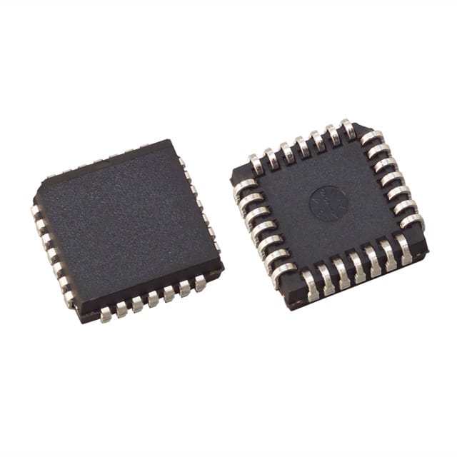
Package
CDCVF111FNRG4 is typically available in a small outline integrated circuit (SOIC) package.
Essence
The essence of CDCVF111FNRG4 lies in its ability to condition digital signals and distribute clock signals efficiently.
Packaging/Quantity
This product is usually packaged in reels or tubes, with a quantity of 250 units per reel/tube.
Specifications and Parameters
- Operating voltage: 3.3V
- Input frequency range: 1 MHz - 200 MHz
- Output frequency range: 1 MHz - 200 MHz
- Number of outputs: 10
- Input/output logic levels: CMOS/TTL compatible
- Operating temperature range: -40°C to +85°C
Pin Configuration
For detailed and complete pin configuration information, please refer to the datasheet provided by the manufacturer.
Functional Characteristics
CDCVF111FNRG4 offers the following functional characteristics:
- Signal conditioning: The IC ensures proper signal shaping and conditioning for reliable transmission.
- Clock distribution: It provides multiple synchronized clock outputs for efficient distribution within a system.
- Frequency multiplication/division: CDCVF111FNRG4 can multiply or divide the input frequency to generate desired clock frequencies.
- Phase-locked loop (PLL): This IC incorporates a PLL circuit for precise clock synchronization and stability.
Advantages and Disadvantages
Advantages
- Efficient signal conditioning and clock distribution
- High-speed operation for fast data processing
- Low power consumption for enhanced energy efficiency
- Compact SOIC package for space-saving designs
Disadvantages
- Limited number of outputs (10)
- Restricted operating temperature range (-40°C to +85°C)
Applicable Range of Products
CDCVF111FNRG4 is widely applicable in various electronic devices that require signal conditioning and clock distribution, such as:
- Communication equipment
- Computer systems
- Consumer electronics
- Industrial automation systems
- Test and measurement instruments
Working Principles
CDCVF111FNRG4 operates based on the principles of signal conditioning and clock distribution. It receives digital signals as inputs, conditions them to ensure reliable transmission, and generates multiple synchronized clock outputs for distribution within a system. The IC utilizes a PLL circuit for precise clock synchronization and stability.
Detailed Application Field Plans
CDCVF111FNRG4 can be utilized in the following application fields:
- Communication Equipment: Used for clock distribution in routers, switches, and network infrastructure devices.
- Computer Systems: Enables clock synchronization and distribution in servers, workstations, and data storage systems.
- Consumer Electronics: Facilitates clock distribution in televisions, audio/video equipment, and gaming consoles.
- Industrial Automation Systems: Provides synchronized clocks for PLCs, motor control systems, and robotics.
- Test and Measurement Instruments: Supports precise timing and synchronization in oscilloscopes, spectrum analyzers, and signal generators.
Detailed Alternative Models
Some alternative models to CDCVF111FNRG4 include:
- CDCVF2505PWR
- CDCVF2509PWR
- CDCVF25081PWR
- CDCVF25081PWG4
- CDCVF25081PW
Please refer to the manufacturer's documentation for detailed specifications and pin configurations of these alternative models.
5 Common Technical Questions and Answers
Q: What is the maximum operating frequency of CDCVF111FNRG4? A: The maximum operating frequency is 200 MHz.
Q: Can CDCVF111FNRG4 be used with both CMOS and TTL logic levels? A: Yes, this IC is compatible with both CMOS and TTL logic levels.
Q: What is the typical power consumption of CDCVF111FNRG4? A: The typical power consumption is low, ensuring energy efficiency in electronic devices.
Q: How many outputs does CDCVF111FNRG4 provide? A: This IC offers 10 synchronized clock outputs.
Q: What is the temperature range within which CDCVF111FNRG4 can operate? A: CDCVF111FNRG4 can operate within