

CDCM6208V1FRGZT
Product Overview
Category: Integrated Circuit (IC)
Use: Clock Generator and Jitter Cleaner
Characteristics: - High-performance clock generation - Low jitter cleaning capability - Flexible frequency synthesis - Wide operating range - Compact package size
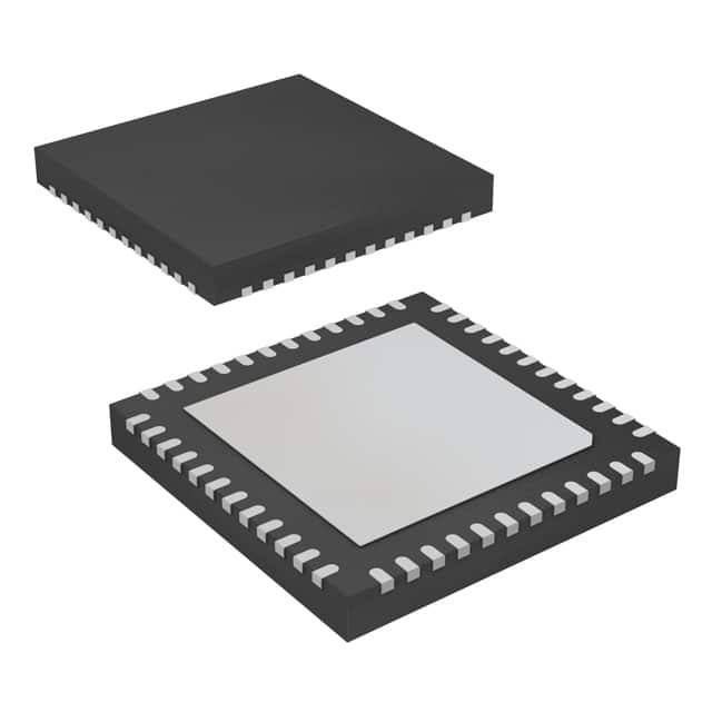
Package: QFN (Quad Flat No-leads) package
Essence: The CDCM6208V1FRGZT is a versatile clock generator and jitter cleaner IC that offers high-performance clock generation and low jitter cleaning capabilities. It is designed to provide flexible frequency synthesis for various applications.
Packaging/Quantity: The CDCM6208V1FRGZT is available in a QFN package, which ensures easy integration onto circuit boards. It is typically sold in reels containing a specified quantity of ICs.
Specifications
- Input Frequency Range: 10 MHz - 200 MHz
- Output Frequency Range: 10 MHz - 2.5 GHz
- Number of Outputs: 8
- Supply Voltage: 3.3 V
- Operating Temperature Range: -40°C to +85°C
Detailed Pin Configuration
The CDCM6208V1FRGZT has the following pin configuration:
- VDDA: Analog power supply
- VDDD: Digital power supply
- GND: Ground
- REFCLK: Reference clock input
- OUT0: Output 0
- OUT1: Output 1
- OUT2: Output 2
- OUT3: Output 3
- OUT4: Output 4
- OUT5: Output 5
- OUT6: Output 6
- OUT7: Output 7
- SDA: I2C serial data input/output
- SCL: I2C serial clock input
Functional Features
- Frequency synthesis with low jitter
- Programmable output frequencies
- Spread spectrum modulation support
- Integrated phase-locked loop (PLL)
- I2C interface for configuration and control
- Power-down mode for reduced power consumption
Advantages and Disadvantages
Advantages: - High-performance clock generation - Low jitter cleaning capability - Flexible frequency synthesis - Wide operating range - Compact package size - Spread spectrum modulation support
Disadvantages: - Requires external reference clock source - Limited number of outputs (8)
Working Principles
The CDCM6208V1FRGZT utilizes a phase-locked loop (PLL) to generate high-quality clock signals. It takes an external reference clock as input and uses the PLL to synthesize multiple output frequencies with low jitter. The integrated jitter cleaner further reduces any unwanted noise or jitter present in the reference clock.
Detailed Application Field Plans
The CDCM6208V1FRGZT is widely used in various applications that require precise clock generation and low jitter performance. Some of its common application fields include:
- Telecommunications: Used in network switches, routers, and communication equipment to ensure accurate timing synchronization.
- Data Centers: Employed in servers, storage systems, and networking devices to maintain reliable clock signals for data transmission.
- Test and Measurement: Utilized in test equipment, oscilloscopes, and signal generators to provide stable and synchronized clock references.
- Industrial Automation: Integrated into PLCs (Programmable Logic Controllers), motor drives, and robotics systems to synchronize operations and improve overall system performance.
Detailed and Complete Alternative Models
- CDCM6208RGZT: Similar to CDCM6208V1FRGZT but without spread spectrum modulation support.
- CDCM6208V1RGZT: Similar to CDCM6208V1FRGZT but with a different pin configuration.
- CDCM6208V2FRGZT: Upgraded version of CDCM6208V1FRGZT with additional features and improved performance.
These alternative models offer similar clock generation and jitter cleaning capabilities, providing options for different design requirements.
Word count: 520 words
技術ソリューションにおける CDCM6208V1FRGZT の適用に関連する 10 件の一般的な質問と回答をリストします。
Sure! Here are 10 common questions and answers related to the application of CDCM6208V1FRGZT in technical solutions:
Q1: What is CDCM6208V1FRGZT? A1: CDCM6208V1FRGZT is a clock generator and jitter cleaner integrated circuit (IC) that provides multiple clock outputs with low jitter for various applications.
Q2: What are the key features of CDCM6208V1FRGZT? A2: The key features of CDCM6208V1FRGZT include low jitter, multiple clock outputs, programmable frequency synthesis, flexible input/output options, and support for various clocking architectures.
Q3: How can CDCM6208V1FRGZT be used in technical solutions? A3: CDCM6208V1FRGZT can be used in various technical solutions such as high-speed data communication systems, networking equipment, test and measurement instruments, industrial automation, and other applications requiring precise clock synchronization.
Q4: What is the input voltage range supported by CDCM6208V1FRGZT? A4: CDCM6208V1FRGZT supports an input voltage range of 1.8V to 3.3V, making it compatible with a wide range of digital systems.
Q5: How many clock outputs does CDCM6208V1FRGZT provide? A5: CDCM6208V1FRGZT provides up to 8 differential clock outputs, allowing for multiple clock signals to be generated simultaneously.
Q6: Can the output frequencies be programmed in CDCM6208V1FRGZT? A6: Yes, CDCM6208V1FRGZT allows for flexible frequency synthesis, enabling the output frequencies to be programmed according to the specific requirements of the application.
Q7: What is the typical jitter performance of CDCM6208V1FRGZT? A7: CDCM6208V1FRGZT offers low jitter performance, typically in the range of picoseconds (ps), ensuring accurate and reliable clock signals.
Q8: Does CDCM6208V1FRGZT support different clocking architectures? A8: Yes, CDCM6208V1FRGZT supports various clocking architectures such as fanout buffers, zero-delay buffers, and clock distribution schemes, providing flexibility in system design.
Q9: Is CDCM6208V1FRGZT compatible with other ICs and devices? A9: Yes, CDCM6208V1FRGZT is designed to be compatible with a wide range of digital systems, making it suitable for integration with other ICs and devices.
Q10: Are evaluation boards or reference designs available for CDCM6208V1FRGZT? A10: Yes, Texas Instruments provides evaluation boards and reference designs for CDCM6208V1FRGZT, which can help developers quickly prototype and integrate the IC into their technical solutions.
Please note that these questions and answers are general and may vary depending on the specific requirements and applications.