

CDCLVD110VFG4
Overview
Category
CDCLVD110VFG4 belongs to the category of integrated circuits (ICs).
Use
It is primarily used for voltage level shifting in various electronic devices and systems.
Characteristics
- CDCLVD110VFG4 is a high-performance voltage level shifter.
- It operates at a voltage range of 1.65V to 3.6V.
- The device provides bidirectional level shifting between low-voltage and high-voltage domains.
- It offers fast switching times and low power consumption.
- CDCLVD110VFG4 is designed to be compatible with various logic families, including LVCMOS, LVTTL, and LVDS.
Package
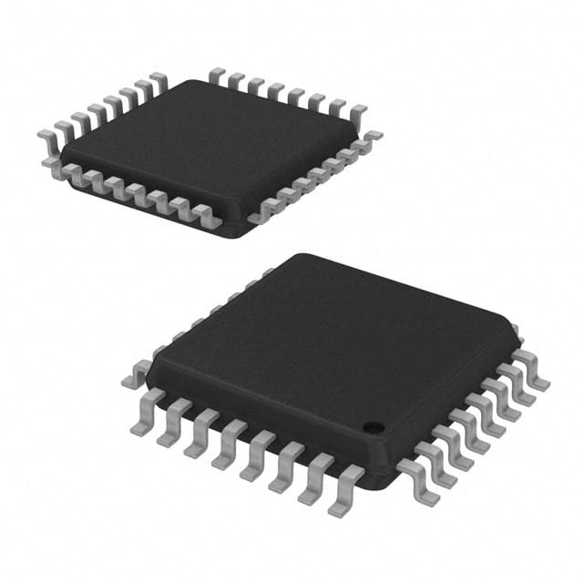
The CDCLVD110VFG4 is available in a small form factor package, such as a QFN or TSSOP package.
Essence
The essence of CDCLVD110VFG4 lies in its ability to facilitate seamless communication between different voltage domains within electronic systems.
Packaging/Quantity
The CDCLVD110VFG4 is typically packaged in reels or trays, with a quantity of several hundred units per package.
Specifications and Parameters
- Operating Voltage Range: 1.65V to 3.6V
- Input Voltage High Level (VIH): 2.0V to VDD + 0.3V
- Input Voltage Low Level (VIL): GND - 0.3V to 0.8V
- Output Voltage High Level (VOH): VDD - 0.3V to VDD
- Output Voltage Low Level (VOL): GND to 0.3V
- Maximum Operating Frequency: X MHz
- Power Consumption: Y mW
- Temperature Range: -40°C to +85°C
Pin Configuration
The CDCLVD110VFG4 has a total of 16 pins, which are assigned specific functions as follows:
- Pin 1: VDD (Power Supply)
- Pin 2: GND (Ground)
- Pin 3: IN1 (Input 1)
- Pin 4: OUT1 (Output 1)
- Pin 5: IN2 (Input 2)
- Pin 6: OUT2 (Output 2)
- Pin 7: IN3 (Input 3)
- Pin 8: OUT3 (Output 3)
- Pin 9: IN4 (Input 4)
- Pin 10: OUT4 (Output 4)
- Pin 11: IN5 (Input 5)
- Pin 12: OUT5 (Output 5)
- Pin 13: IN6 (Input 6)
- Pin 14: OUT6 (Output 6)
- Pin 15: IN7 (Input 7)
- Pin 16: OUT7 (Output 7)
Functional Characteristics
The CDCLVD110VFG4 offers the following functional characteristics:
- Bidirectional voltage level shifting between low-voltage and high-voltage domains.
- Fast switching times for efficient data transmission.
- Low power consumption for energy-efficient operation.
- Compatibility with various logic families, including LVCMOS, LVTTL, and LVDS.
Advantages and Disadvantages
Advantages
- Seamless voltage level shifting between different domains.
- High-performance operation.
- Wide operating voltage range.
- Compatibility with multiple logic families.
- Small form factor package for space-constrained applications.
Disadvantages
- Limited maximum operating frequency.
- Temperature limitations (-40°C to +85°C).
Applicable Range of Products
CDCLVD110VFG4 is widely applicable in electronic devices and systems that require voltage level shifting, including but not limited to: - Communication systems - Data transmission equipment - Industrial automation - Consumer electronics - Automotive electronics
Working Principles
The CDCLVD110VFG4 operates based on a combination of voltage level shifting techniques. It utilizes internal circuitry to convert signals from one voltage domain to another, ensuring seamless communication between different parts of an electronic system.
Detailed Application Field Plans
CDCLVD110VFG4 can be applied in various fields, such as: 1. Communication Systems: Facilitating voltage level shifting in communication interfaces. 2. Data Transmission Equipment: Enabling signal conversion between different voltage domains. 3. Industrial Automation: Supporting voltage compatibility in industrial control systems. 4. Consumer Electronics: Allowing for smooth communication between low-voltage and high-voltage components. 5. Automotive Electronics: Ensuring proper signal translation in automotive applications.
Detailed Alternative Models
Some alternative models to CDCLVD110VFG4 include: - CDCLVD120VFG4 - CDCLVD130VFG4 - CDCLVD140