

CD74AC540ME4
Product Overview
- Category: Integrated Circuit
- Use: Logic Level Shifter
- Characteristics: High-speed, low-power consumption
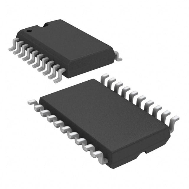
- Package: SOIC (Small Outline Integrated Circuit)
- Essence: The CD74AC540ME4 is a logic level shifter integrated circuit that allows for bidirectional voltage translation between different logic levels.
- Packaging/Quantity: Available in tape and reel packaging with 2500 units per reel.
Specifications
- Supply Voltage: 2V to 6V
- Logic Family: AC
- Number of Channels: 8
- Input/Output Compatibility: TTL/CMOS
- Propagation Delay: 5.5ns (typical)
- Operating Temperature Range: -40°C to +85°C
Detailed Pin Configuration
The CD74AC540ME4 has a total of 20 pins, which are arranged as follows:
__    __
   A1 |1  \__/ 20| VCC
   B1 |2        19| OE#
   A2 |3        18| I/O1
   B2 |4        17| I/O2
   A3 |5        16| I/O3
   B3 |6        15| I/O4
   A4 |7        14| I/O5
   B4 |8   CD   13| I/O6
  GND |9   74   12| I/O7
   OE |10  AC   11| I/O8
       --    --
Functional Features
- Bidirectional voltage translation: Allows for seamless communication between devices operating at different logic levels.
- High-speed operation: The CD74AC540ME4 offers fast propagation delay, making it suitable for high-frequency applications.
- Low-power consumption: Designed to minimize power consumption, making it ideal for battery-powered devices.
- Output enable (OE) control: The OE pin allows the user to disable the outputs when not in use, reducing power consumption and preventing bus contention.
Advantages and Disadvantages
Advantages
- Efficient voltage level shifting between different logic families.
- High-speed operation enables reliable data transmission in time-critical applications.
- Low-power consumption extends battery life in portable devices.
- Output enable feature provides flexibility in controlling the device's output state.
Disadvantages
- Limited number of channels (8) may not be sufficient for complex systems requiring a higher number of inputs/outputs.
- Operating temperature range (-40°C to +85°C) may not be suitable for extreme environments.
Working Principles
The CD74AC540ME4 utilizes a combination of MOSFETs and CMOS technology to achieve bidirectional voltage translation. It employs a voltage level shifting technique that allows seamless communication between devices operating at different logic levels. The device operates by monitoring the input voltage levels and translating them to the desired output voltage levels based on the logic family compatibility.
Detailed Application Field Plans
The CD74AC540ME4 is commonly used in various applications, including:
- Microcontroller Interfacing: It facilitates communication between microcontrollers operating at different logic levels, enabling seamless integration into complex systems.
- Data Communication: The CD74AC540ME4 is widely used in data communication systems, such as UART (Universal Asynchronous Receiver-Transmitter) interfaces, where voltage level translation is required.
- Sensor Interfaces: It serves as an interface between sensors and microcontrollers, allowing for accurate data acquisition and processing.
- Industrial Automation: The CD74AC540ME4 finds application in industrial automation systems, where it enables communication between different control modules operating at different voltage levels.
Detailed and Complete Alternative Models
- SN74LVC245A: This logic level shifter offers similar functionality with a wider operating temperature range (-55°C to +125°C) and a higher number of channels (16).
- CD4050B: This CMOS-based logic level shifter provides bidirectional voltage translation with a wide supply voltage range (3V to 18V) and a higher number of channels (6).
These alternative models can be considered based on specific application requirements and environmental conditions.
Word count: 496 words
技術ソリューションにおける CD74AC540ME4 の適用に関連する 10 件の一般的な質問と回答をリストします。
Sure! Here are 10 common questions and answers related to the application of CD74AC540ME4 in technical solutions:
Q: What is CD74AC540ME4? A: CD74AC540ME4 is a type of octal buffer/line driver integrated circuit (IC) that is commonly used in digital electronic systems.
Q: What is the purpose of CD74AC540ME4? A: The purpose of CD74AC540ME4 is to provide buffering and line driving capabilities for digital signals, allowing them to be transmitted over longer distances or to multiple devices.
Q: What voltage levels does CD74AC540ME4 support? A: CD74AC540ME4 supports a wide range of voltage levels, typically between 2V and 6V.
Q: How many input/output pins does CD74AC540ME4 have? A: CD74AC540ME4 has 8 input pins and 8 output pins, making it an octal device.
Q: Can CD74AC540ME4 handle bidirectional communication? A: Yes, CD74AC540ME4 can handle bidirectional communication by using its direction control pin.
Q: What is the maximum operating frequency of CD74AC540ME4? A: CD74AC540ME4 has a maximum operating frequency of typically around 100 MHz.
Q: Does CD74AC540ME4 have any built-in protection features? A: Yes, CD74AC540ME4 has built-in ESD (electrostatic discharge) protection on its inputs and outputs to prevent damage from static electricity.
Q: Can CD74AC540ME4 drive capacitive loads? A: Yes, CD74AC540ME4 can drive capacitive loads up to a certain limit, typically around 50 pF.
Q: What is the power supply voltage range for CD74AC540ME4? A: CD74AC540ME4 operates with a power supply voltage range of typically between 2V and 6V.
Q: Can CD74AC540ME4 be used in automotive applications? A: Yes, CD74AC540ME4 is suitable for use in automotive applications as it meets the necessary standards and requirements.
Please note that the answers provided here are general and may vary depending on specific datasheet specifications and application requirements.