

ADCS9888CVH-140/NOPB
Overview
- Category: Integrated Circuit (IC)
- Use: Analog-to-Digital Converter (ADC)
- Characteristics: High-speed, high-resolution ADC
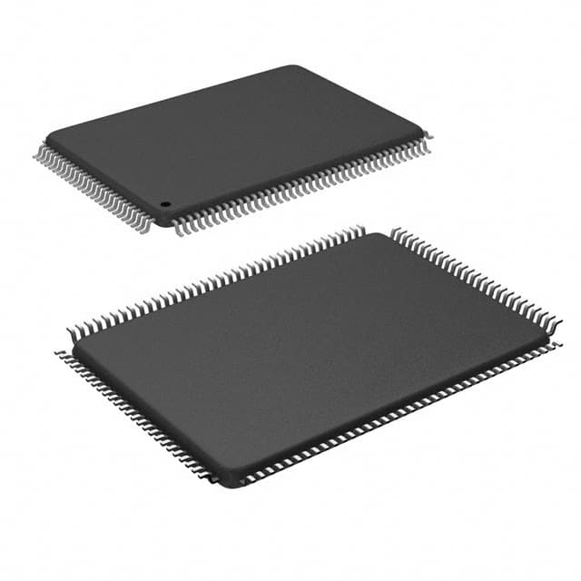
- Package: Ceramic Quad Flatpack (CQFP)
- Essence: Converts analog signals to digital data
- Packaging/Quantity: Single unit per package
Specifications
- Resolution: 14 bits
- Sampling Rate: Up to 100 MSPS (Mega Samples Per Second)
- Input Voltage Range: ±2 V
- Power Supply: +5 V
- Operating Temperature Range: -40°C to +85°C
Pin Configuration
The ADCS9888CVH-140/NOPB has a total of 48 pins. The pin configuration is as follows:
- VREFP
- VREFN
- AGND
- AVDD
- DVDD
- DGND
- CLKIN
- CLKOUT
- PDWN
- RESET
- CS
- SCLK
- SDATA
- D0
- D1
- D2
- D3
- D4
- D5
- D6
- D7
- D8
- D9
- D10
- D11
- D12
- D13
- D14
- D15
- D16
- D17
- D18
- D19
- D20
- D21
- D22
- D23
- D24
- D25
- D26
- D27
- D28
- D29
- D30
- D31
- D32
- D33
- D34
Functional Features
- High-speed conversion of analog signals to digital data
- 14-bit resolution provides accurate representation of input signals
- Wide input voltage range allows for versatile applications
- Low power consumption for energy-efficient operation
- Compact package size for space-constrained designs
Advantages and Disadvantages
Advantages: - High-resolution conversion - Fast sampling rate - Wide input voltage range - Low power consumption
Disadvantages: - Limited number of input channels - Requires external clock signal
Working Principles
The ADCS9888CVH-140/NOPB operates by sampling the analog input voltage and converting it into a digital representation using a successive approximation algorithm. The input voltage is compared to a reference voltage, and the resulting digital code represents the magnitude of the input signal. The conversion process is controlled by the internal clock signal and can be initiated by the user.
Detailed Application Field Plans
The ADCS9888CVH-140/NOPB is commonly used in various applications that require high-speed and high-resolution analog-to-digital conversion. Some potential application fields include: - Communications systems - Medical imaging equipment - Test and measurement instruments - Industrial automation - Audio and video processing
Alternative Models
Here are some alternative models that offer similar functionality to the ADCS9888CVH-140/NOPB: - ADCS9888CVH-120/NOPB: 12-bit resolution, lower cost - ADCS9888CVH-160/NOPB: 16-bit resolution, higher accuracy - ADCS9888CVH-200/NOPB: 20-bit resolution, ultra-high precision
Please note that the specifications and pin configuration may vary for each alternative model.
This entry has provided an overview of the ADCS9888CVH-140/NOPB, including its basic information, specifications, pin configuration, functional features, advantages and disadvantages, working principles, detailed application field plans, and alternative models.
技術ソリューションにおける ADCS9888CVH-140/NOPB の適用に関連する 10 件の一般的な質問と回答をリストします。
Question: What is the ADCS9888CVH-140/NOPB?
Answer: The ADCS9888CVH-140/NOPB is a high-performance analog-to-digital converter (ADC) designed for use in technical solutions.Question: What is the resolution of the ADCS9888CVH-140/NOPB?
Answer: The ADCS9888CVH-140/NOPB has a resolution of 14 bits, allowing for precise and accurate conversion of analog signals to digital values.Question: What is the sampling rate of the ADCS9888CVH-140/NOPB?
Answer: The ADCS9888CVH-140/NOPB has a maximum sampling rate of 140 mega-samples per second (MSPS), enabling fast and efficient data acquisition.Question: What is the input voltage range of the ADCS9888CVH-140/NOPB?
Answer: The ADCS9888CVH-140/NOPB has a wide input voltage range of -0.5V to +1.5V, making it suitable for a variety of signal levels.Question: Does the ADCS9888CVH-140/NOPB support differential inputs?
Answer: Yes, the ADCS9888CVH-140/NOPB supports both single-ended and differential inputs, providing flexibility in signal connection.Question: What is the power supply voltage requirement for the ADCS9888CVH-140/NOPB?
Answer: The ADCS9888CVH-140/NOPB requires a power supply voltage of +3.3V, ensuring compatibility with standard power sources.Question: Can the ADCS9888CVH-140/NOPB be used in low-power applications?
Answer: Yes, the ADCS9888CVH-140/NOPB features a power-down mode, allowing for reduced power consumption when not actively converting signals.Question: Does the ADCS9888CVH-140/NOPB provide any built-in digital signal processing (DSP) features?
Answer: No, the ADCS9888CVH-140/NOPB is a standalone ADC and does not include any built-in DSP functionality.Question: What is the interface used to communicate with the ADCS9888CVH-140/NOPB?
Answer: The ADCS9888CVH-140/NOPB utilizes a parallel interface for data transfer, providing fast and efficient communication with external devices.Question: Are evaluation boards or reference designs available for the ADCS9888CVH-140/NOPB?
Answer: Yes, Texas Instruments provides evaluation boards and reference designs for the ADCS9888CVH-140/NOPB, facilitating easy integration into technical solutions.