

74SSTUB32865ZJBR
Basic Information Overview
- Category: Integrated Circuit (IC)
- Use: Digital Logic Device
- Characteristics: High-speed, Low-power, TTL-compatible
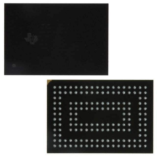
- Package: Surface Mount Technology (SMT)
- Essence: Flip-Flop Register
- Packaging/Quantity: Tape and Reel, 2500 units per reel
Specifications
- Supply Voltage: 3.3V
- Logic Family: SSTL (Stub Series Terminated Logic)
- Number of Flip-Flops: 8
- Maximum Clock Frequency: 500 MHz
- Operating Temperature Range: -40°C to +85°C
Detailed Pin Configuration
- CLK (Clock Input)
- D0-D7 (Data Inputs)
- Q0-Q7 (Flip-Flop Outputs)
- GND (Ground)
- VCC (Power Supply)
Functional Features
- High-speed operation allows for efficient data processing.
- Low-power consumption ensures energy efficiency.
- TTL compatibility enables easy integration with existing systems.
- Flip-flop outputs provide stable storage of data.
Advantages
- Fast data transfer rates enhance system performance.
- Low power consumption reduces energy costs.
- Compatibility with TTL logic simplifies system design.
- Reliable flip-flop outputs ensure accurate data storage.
Disadvantages
- Limited voltage supply range (3.3V) may not be suitable for all applications.
- Higher cost compared to some alternative models.
- SMT packaging may require specialized equipment for assembly.
Working Principles
The 74SSTUB32865ZJBR is a flip-flop register that stores and transfers digital data. It operates on a clock signal, which synchronizes the input data with the internal flip-flops. The data inputs (D0-D7) are captured and stored in the flip-flops when a rising edge is detected on the clock input (CLK). The stored data can then be accessed from the flip-flop outputs (Q0-Q7).
Detailed Application Field Plans
The 74SSTUB32865ZJBR is commonly used in various applications, including: 1. Communication Systems: Data transmission and reception. 2. Computer Networks: Buffering and routing of data packets. 3. Industrial Automation: Control and monitoring of processes. 4. Consumer Electronics: High-speed data processing in multimedia devices. 5. Automotive Electronics: Signal conditioning and control systems.
Detailed and Complete Alternative Models
- 74HC595: 8-bit shift register with serial input and parallel output.
- CD4015: Dual 4-stage static shift register with parallel input and serial output.
- SN74LS164: 8-bit serial-in/parallel-out shift register.
Please note that these alternative models may have different specifications and pin configurations, so careful consideration should be given to their compatibility with specific applications.
Word count: 324 words
技術ソリューションにおける 74SSTUB32865ZJBR の適用に関連する 10 件の一般的な質問と回答をリストします。
Sure! Here are 10 common questions and answers related to the application of 74SSTUB32865ZJBR in technical solutions:
Q: What is the purpose of the 74SSTUB32865ZJBR integrated circuit? A: The 74SSTUB32865ZJBR is a high-speed, low-power 32-bit bus transceiver with 3-state outputs. It is designed for use in various digital communication and data processing applications.
Q: What voltage levels does the 74SSTUB32865ZJBR support? A: The 74SSTUB32865ZJBR supports voltage levels of 3.3V, making it compatible with many modern digital systems.
Q: Can the 74SSTUB32865ZJBR be used as a bidirectional transceiver? A: Yes, the 74SSTUB32865ZJBR is a bidirectional transceiver, allowing data to be transmitted and received on the same set of pins.
Q: What is the maximum data transfer rate supported by the 74SSTUB32865ZJBR? A: The 74SSTUB32865ZJBR can support data transfer rates of up to several hundred megabits per second, depending on the specific application and system configuration.
Q: Does the 74SSTUB32865ZJBR have built-in protection features? A: Yes, the 74SSTUB32865ZJBR includes built-in ESD (electrostatic discharge) protection on its I/O pins, helping to safeguard against damage from static electricity.
Q: Can the 74SSTUB32865ZJBR be used in hot-swappable applications? A: Yes, the 74SSTUB32865ZJBR supports hot-swapping, allowing it to be inserted or removed from a live system without causing damage.
Q: What is the power consumption of the 74SSTUB32865ZJBR? A: The power consumption of the 74SSTUB32865ZJBR is relatively low, making it suitable for battery-powered devices and energy-efficient applications.
Q: Does the 74SSTUB32865ZJBR have any specific timing requirements? A: Yes, the 74SSTUB32865ZJBR has specific timing requirements for proper operation. These timings are outlined in the datasheet and should be followed for reliable performance.
Q: Can the 74SSTUB32865ZJBR be cascaded with other transceivers? A: Yes, multiple 74SSTUB32865ZJBR transceivers can be cascaded together to expand the number of bidirectional data lines in a system.
Q: Are there any known limitations or considerations when using the 74SSTUB32865ZJBR? A: While the 74SSTUB32865ZJBR is a versatile transceiver, it is important to consider factors such as signal integrity, noise immunity, and proper decoupling to ensure optimal performance in specific applications.