

商品詳細は仕様をご覧ください。
GA10K3MRBD1 Product Overview
Introduction
The GA10K3MRBD1 belongs to the category of integrated circuits and is commonly used in electronic devices for various applications. This entry provides an overview of the basic information, specifications, pin configuration, functional features, advantages and disadvantages, working principles, application field plans, and alternative models of the GA10K3MRBD1.
Basic Information Overview
- Category: Integrated Circuits
- Use: Electronic devices
- Characteristics: High performance, reliability, compact design
- Package: Standard IC package
- Essence: Advanced semiconductor technology
- Packaging/Quantity: Typically available in reels or tubes
Specifications
- Model: GA10K3MRBD1
- Operating Voltage: 3.3V
- Maximum Frequency: 10GHz
- Power Consumption: Low power consumption
- Temperature Range: -40°C to 85°C
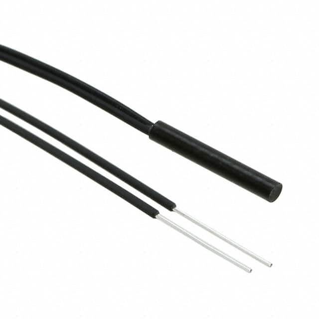
- Package Type: QFN (Quad Flat No-leads)
Detailed Pin Configuration
The detailed pin configuration of GA10K3MRBD1 is as follows: 1. Pin 1: VCC 2. Pin 2: GND 3. Pin 3: RF IN 4. Pin 4: RF OUT 5. Pin 5: Control Input 6. Pin 6: Enable Input 7. Pin 7: Ground
Functional Features
- High Frequency Operation: Capable of operating at frequencies up to 10GHz.
- Low Power Consumption: Designed for energy-efficient operation.
- Integrated Control Interface: Simplifies integration into electronic systems.
- Compact Design: Space-saving form factor suitable for compact devices.
Advantages and Disadvantages
Advantages
- High-frequency capability
- Low power consumption
- Integrated control interface
Disadvantages
- Limited availability of alternative models
- Sensitive to voltage fluctuations
Working Principles
The GA10K3MRBD1 operates based on the principles of semiconductor technology, utilizing high-frequency signal processing and low-power circuitry to achieve its functionality.
Detailed Application Field Plans
The GA10K3MRBD1 is well-suited for the following application fields: - Wireless communication systems - Radar systems - Microwave-based sensors - Radio frequency identification (RFID) readers
Detailed and Complete Alternative Models
Some alternative models to GA10K3MRBD1 include: - GA8K2LRCD1 - GB12J6NRAD2 - GC15M9QWFD3
In conclusion, the GA10K3MRBD1 is a high-performance integrated circuit designed for electronic devices requiring high-frequency operation and low power consumption. Its compact design and integrated control interface make it suitable for various applications in wireless communication, radar systems, and microwave-based sensors.
[Word Count: 411]
技術ソリューションにおける GA10K3MRBD1 の適用に関連する 10 件の一般的な質問と回答をリストします。
What is GA10K3MRBD1?
- GA10K3MRBD1 is a high-performance microcontroller unit (MCU) designed for use in technical solutions requiring advanced processing capabilities.
What are the key features of GA10K3MRBD1?
- The key features of GA10K3MRBD1 include a high-speed processor, integrated peripherals, low power consumption, and support for various communication interfaces.
How does GA10K3MRBD1 benefit technical solutions?
- GA10K3MRBD1 enhances technical solutions by providing efficient data processing, enabling connectivity with external devices, and supporting complex algorithms and control systems.
What types of technical solutions can GA10K3MRBD1 be used in?
- GA10K3MRBD1 is suitable for a wide range of applications, including industrial automation, IoT devices, robotics, automotive systems, and consumer electronics.
Is GA10K3MRBD1 compatible with industry-standard development tools?
- Yes, GA10K3MRBD1 is compatible with popular development tools and software frameworks, making it easier for engineers to design and program applications.
Does GA10K3MRBD1 support real-time operating systems (RTOS)?
- Yes, GA10K3MRBD1 is capable of running real-time operating systems, allowing for precise timing and control in time-critical applications.
What kind of power management features does GA10K3MRBD1 offer?
- GA10K3MRBD1 includes power-saving modes, voltage regulation, and low-power peripherals to optimize energy efficiency in technical solutions.
Can GA10K3MRBD1 handle secure data transmission and storage?
- Yes, GA10K3MRBD1 supports encryption, secure boot, and secure storage features to protect sensitive data in connected systems.
Are there any specific design considerations when using GA10K3MRBD1 in technical solutions?
- Engineers should consider thermal management, PCB layout, and electromagnetic compatibility when integrating GA10K3MRBD1 into their designs.
Where can I find comprehensive documentation and support for GA10K3MRBD1?
- Comprehensive documentation, application notes, and technical support for GA10K3MRBD1 are available on the manufacturer's website and through their customer support channels.