

TSV911IDT
Product Overview
Category
TSV911IDT belongs to the category of integrated circuits (ICs).
Use
The TSV911IDT is commonly used as an operational amplifier (op-amp) in various electronic applications.
Characteristics
- High gain and bandwidth
- Low input offset voltage
- Low power consumption
- Rail-to-rail input and output capability
Package
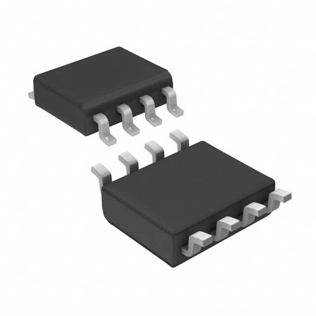
The TSV911IDT is available in a small outline package (SOT-23) which provides ease of integration into compact circuit designs.
Essence
The essence of TSV911IDT lies in its ability to amplify and process analog signals with high precision and efficiency.
Packaging/Quantity
The TSV911IDT is typically packaged in reels, containing a quantity of 3000 units per reel.
Specifications
- Supply Voltage: ±2.5V to ±6V
- Input Offset Voltage: 1mV (maximum)
- Gain Bandwidth Product: 10MHz (typical)
- Slew Rate: 3V/µs (typical)
- Quiescent Current: 500µA (typical)
Detailed Pin Configuration
The TSV911IDT has a total of 5 pins arranged as follows:
```
| | --| IN- OUT |-- --| IN+ VCC |-- --| GND NC |-- |___________| ```
Pin Description: - IN-: Inverting input - IN+: Non-inverting input - OUT: Output - VCC: Positive supply voltage - GND: Ground - NC: No connection
Functional Features
- High Gain: The TSV911IDT offers a high open-loop voltage gain, allowing for accurate signal amplification.
- Wide Bandwidth: With a gain bandwidth product of 10MHz, it can handle high-frequency signals effectively.
- Low Input Offset Voltage: The op-amp exhibits minimal voltage difference between its input terminals, ensuring precise signal processing.
- Rail-to-Rail I/O: The TSV911IDT supports input and output signals that can swing close to the supply rails, maximizing dynamic range.
Advantages and Disadvantages
Advantages
- High gain and bandwidth enable accurate signal amplification.
- Low input offset voltage ensures precise signal processing.
- Rail-to-rail I/O capability allows for maximum dynamic range.
- Low power consumption contributes to energy efficiency.
Disadvantages
- Limited supply voltage range (±2.5V to ±6V).
- Slightly lower slew rate compared to some alternative models.
Working Principles
The TSV911IDT operates based on the principles of differential amplification. It amplifies the voltage difference between its inverting and non-inverting inputs, producing an amplified output signal. The op-amp's internal circuitry, including transistors and resistors, facilitates this amplification process.
Detailed Application Field Plans
The TSV911IDT finds applications in various fields, including: 1. Audio Amplification: It can be used in audio systems to amplify low-level audio signals with high fidelity. 2. Sensor Signal Conditioning: The op-amp can be employed to amplify and condition weak sensor signals for further processing. 3. Active Filters: It is suitable for implementing active filters in communication systems, allowing for precise frequency response shaping. 4. Instrumentation Amplifiers: The TSV911IDT can be utilized as a building block for instrumentation amplifiers, enhancing measurement accuracy.
Detailed and Complete Alternative Models
Some alternative models to the TSV911IDT include: 1. LM358: A dual operational amplifier with similar characteristics. 2. MCP6001: A low-power op-amp with rail-to-rail input and output capability. 3. TL071: A high-performance JFET-input operational amplifier.
These alternative models offer similar functionalities and can be considered based on specific application requirements.
Word count: 533 words
技術ソリューションにおける TSV911IDT の適用に関連する 10 件の一般的な質問と回答をリストします。
Sure! Here are 10 common questions and answers related to the application of TSV911IDT in technical solutions:
Q: What is TSV911IDT? A: TSV911IDT is a high-speed operational amplifier (op-amp) designed for various technical applications.
Q: What are the key features of TSV911IDT? A: TSV911IDT offers low input bias current, low offset voltage, high slew rate, and wide bandwidth, making it suitable for precision signal conditioning and amplification.
Q: What is the typical voltage supply range for TSV911IDT? A: TSV911IDT operates on a typical voltage supply range of ±2.5V to ±18V.
Q: Can TSV911IDT be used in single-supply applications? A: Yes, TSV911IDT can be used in single-supply applications by connecting the negative supply pin to ground.
Q: What is the maximum output current capability of TSV911IDT? A: The maximum output current capability of TSV911IDT is typically around 40mA.
Q: Is TSV911IDT suitable for low-power applications? A: Yes, TSV911IDT has a low quiescent current consumption, making it suitable for low-power applications.
Q: Can TSV911IDT operate in high-temperature environments? A: Yes, TSV911IDT has a wide operating temperature range of -40°C to +125°C, allowing it to function in high-temperature environments.
Q: What are some common applications of TSV911IDT? A: TSV911IDT is commonly used in audio amplifiers, sensor interfaces, data acquisition systems, and other precision measurement applications.
Q: Does TSV911IDT have built-in protection features? A: Yes, TSV911IDT includes built-in protection against overvoltage, short circuits, and thermal shutdown to ensure safe operation.
Q: Is TSV911IDT available in different package options? A: Yes, TSV911IDT is available in various package options, including SOIC, SOT23, and DFN, providing flexibility for different PCB layouts and space constraints.
Please note that the answers provided here are general and may vary depending on the specific datasheet and manufacturer's specifications of TSV911IDT.