

TSV358IYDT
Product Overview
Category
TSV358IYDT belongs to the category of integrated circuits (ICs).
Use
This IC is commonly used in electronic devices for signal amplification and processing.
Characteristics
- TSV358IYDT is a low-power, rail-to-rail input/output operational amplifier.
- It operates on a single supply voltage ranging from 2.7V to 5.5V.
- The IC has a wide bandwidth of 1 MHz and a low input offset voltage of 1 mV.
- It offers a high slew rate of 0.6 V/μs and a low quiescent current of 50 μA.
- TSV358IYDT is designed for applications requiring precision and low power consumption.
Package
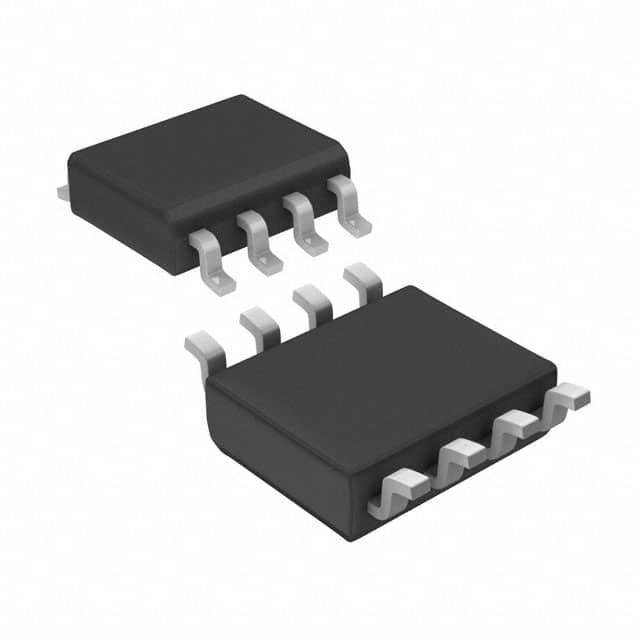
The TSV358IYDT IC is available in a small outline package (SOP) with eight pins.
Essence
The essence of TSV358IYDT lies in its ability to provide accurate and efficient signal amplification while consuming minimal power.
Packaging/Quantity
The IC is typically sold in reels or tubes containing multiple units. The exact quantity depends on the supplier and customer requirements.
Specifications
- Supply Voltage: 2.7V - 5.5V
- Input Offset Voltage: 1 mV
- Bandwidth: 1 MHz
- Slew Rate: 0.6 V/μs
- Quiescent Current: 50 μA
- Package Type: SOP-8
Detailed Pin Configuration
The TSV358IYDT IC has the following pin configuration:
- OUT: Output pin
- IN-: Inverting input pin
- IN+: Non-inverting input pin
- V-: Negative power supply pin
- NC: No connection pin
- V+: Positive power supply pin
- NC: No connection pin
- GND: Ground pin
Functional Features
- Rail-to-rail input/output capability allows for maximum dynamic range.
- Low quiescent current enables power-efficient operation.
- High slew rate ensures fast signal response.
- Wide bandwidth facilitates accurate signal amplification and processing.
Advantages and Disadvantages
Advantages
- Low power consumption
- Rail-to-rail operation
- Accurate signal amplification
- Small package size
Disadvantages
- Limited bandwidth compared to some other ICs in the same category
- May not be suitable for high-frequency applications
Working Principles
The TSV358IYDT operates as an operational amplifier, amplifying and processing input signals. It utilizes a rail-to-rail input/output architecture, allowing it to handle signals close to its supply voltage levels. The IC's low quiescent current ensures minimal power consumption during operation.
Detailed Application Field Plans
TSV358IYDT finds application in various electronic devices and systems, including but not limited to: - Audio amplifiers - Sensor interfaces - Battery-powered devices - Portable instrumentation - Signal conditioning circuits
Detailed and Complete Alternative Models
Some alternative models that offer similar functionality to TSV358IYDT include: - LM324 - MCP6004 - TLV2462 - AD8605
These alternatives can be considered based on specific requirements and design constraints.
Word count: 440 words
技術ソリューションにおける TSV358IYDT の適用に関連する 10 件の一般的な質問と回答をリストします。
Sure! Here are 10 common questions and answers related to the application of TSV358IYDT in technical solutions:
Q: What is TSV358IYDT? A: TSV358IYDT is a specific model or type of electronic component used in technical solutions.
Q: What is the purpose of TSV358IYDT? A: TSV358IYDT is typically used as an operational amplifier (op-amp) in various electronic circuits.
Q: What are the key features of TSV358IYDT? A: Some key features of TSV358IYDT include low power consumption, high gain bandwidth product, and rail-to-rail input/output capability.
Q: In what applications can TSV358IYDT be used? A: TSV358IYDT can be used in a wide range of applications such as audio amplifiers, sensor interfaces, signal conditioning circuits, and active filters.
Q: What is the voltage supply range for TSV358IYDT? A: TSV358IYDT typically operates with a voltage supply range of 2.7V to 5.5V.
Q: What is the maximum output current of TSV358IYDT? A: The maximum output current of TSV358IYDT is typically around 40mA.
Q: Can TSV358IYDT operate in both single-supply and dual-supply configurations? A: Yes, TSV358IYDT can operate in both single-supply and dual-supply configurations, making it versatile for different design requirements.
Q: What is the input offset voltage of TSV358IYDT? A: The input offset voltage of TSV358IYDT is typically very low, around a few microvolts.
Q: Is TSV358IYDT available in surface mount packages? A: Yes, TSV358IYDT is commonly available in surface mount packages such as SOIC and SOT-23.
Q: Are there any recommended application circuits or reference designs for TSV358IYDT? A: Yes, the datasheet of TSV358IYDT usually provides recommended application circuits and reference designs to help users get started with their specific applications.
Please note that the specific details mentioned above may vary depending on the manufacturer and version of TSV358IYDT.