

STW9NK70Z
Introduction
The STW9NK70Z is a power MOSFET belonging to the category of semiconductor devices. It is widely used in various electronic applications due to its unique characteristics and performance. This entry provides an overview of the STW9NK70Z, including its basic information, specifications, pin configuration, functional features, advantages and disadvantages, working principles, application field plans, and alternative models.
Basic Information Overview
- Category: Semiconductor device
- Use: Power MOSFET for electronic applications
- Characteristics: High voltage capability, low on-resistance, fast switching speed
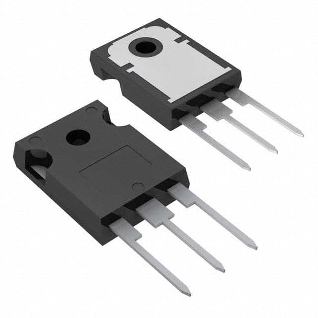
- Package: TO-247
- Essence: Power management
- Packaging/Quantity: Typically available in reels or tubes containing multiple units
Specifications
- Voltage Rating: 700V
- Current Rating: 9A
- On-Resistance: 1.3Ω
- Gate Charge: 28nC
- Operating Temperature Range: -55°C to 150°C
- Datasheet: STW9NK70Z Datasheet
Detailed Pin Configuration
The STW9NK70Z features a standard TO-247 pin configuration with the following pins: 1. Gate (G): Control terminal for turning the MOSFET on and off 2. Source (S): Connection to the ground or common reference point 3. Drain (D): Output terminal for the load
Functional Features
- High Voltage Capability: Suitable for high voltage applications
- Low On-Resistance: Minimizes power losses and improves efficiency
- Fast Switching Speed: Enables rapid switching operations in electronic circuits
Advantages and Disadvantages
Advantages
- Efficient power management
- High voltage handling capability
- Low conduction losses
Disadvantages
- Sensitivity to static electricity
- Gate drive complexity in some applications
Working Principles
The STW9NK70Z operates based on the principle of field-effect transistors. When a suitable voltage is applied to the gate terminal, it creates an electric field that controls the flow of current between the source and drain terminals. This mechanism enables efficient power switching and control in electronic circuits.
Detailed Application Field Plans
The STW9NK70Z finds extensive use in the following application fields: - Switched Mode Power Supplies (SMPS) - Motor Control Systems - Lighting Ballasts - Electronic Inverters - Industrial Automation
Detailed and Complete Alternative Models
- STW8NK80Z: Similar power MOSFET with lower on-resistance
- STW10NK80Z: Higher voltage rating variant for specific applications
- IRF840: Alternative MOSFET from a different manufacturer with comparable specifications
In conclusion, the STW9NK70Z power MOSFET offers high voltage capability, low on-resistance, and fast switching speed, making it suitable for diverse electronic applications such as SMPS, motor control systems, and lighting ballasts. While it has advantages in power management and voltage handling, it may require careful handling due to sensitivity to static electricity. Understanding its specifications, pin configuration, functional features, and alternative models is essential for effective utilization in electronic designs.
[Word Count: 498]
技術ソリューションにおける STW9NK70Z の適用に関連する 10 件の一般的な質問と回答をリストします。
What is the maximum drain-source voltage (VDS) of STW9NK70Z?
- The maximum drain-source voltage (VDS) of STW9NK70Z is 700V.
What is the continuous drain current (ID) rating of STW9NK70Z?
- The continuous drain current (ID) rating of STW9NK70Z is 9A.
What is the on-state resistance (RDS(on)) of STW9NK70Z?
- The on-state resistance (RDS(on)) of STW9NK70Z is typically 1.5 ohms.
What is the gate threshold voltage (VGS(th)) of STW9NK70Z?
- The gate threshold voltage (VGS(th)) of STW9NK70Z is typically 3V.
What are the typical applications for STW9NK70Z?
- STW9NK70Z is commonly used in applications such as switch mode power supplies, electronic lamp ballasts, and motor control circuits.
What is the maximum junction temperature (Tj) of STW9NK70Z?
- The maximum junction temperature (Tj) of STW9NK70Z is 150°C.
Does STW9NK70Z have built-in protection features?
- Yes, STW9NK70Z has built-in protection features such as thermal shutdown and overcurrent protection.
What is the input capacitance (Ciss) of STW9NK70Z?
- The input capacitance (Ciss) of STW9NK70Z is typically 1100pF.
Is STW9NK70Z suitable for high-frequency switching applications?
- Yes, STW9NK70Z is suitable for high-frequency switching applications due to its low on-state resistance and fast switching characteristics.
What are the recommended operating conditions for STW9NK70Z?
- The recommended operating conditions for STW9NK70Z include a maximum drain-source voltage (VDS) of 700V, a continuous drain current (ID) within the specified range, and a junction temperature (Tj) below the maximum limit.