

STW50NB20
Introduction
The STW50NB20 is a power MOSFET belonging to the category of semiconductor devices. It is commonly used in electronic circuits for various applications due to its specific characteristics and performance.
Basic Information Overview
- Category: Semiconductor device
- Use: Power switching applications
- Characteristics: High voltage capability, low on-resistance, fast switching speed
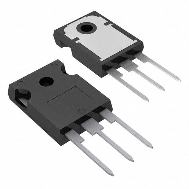
- Package: TO-247
- Essence: Power MOSFET for high-performance applications
- Packaging/Quantity: Typically sold individually or in reels
Specifications
- Voltage Rating: 500V
- Current Rating: 50A
- On-Resistance: 0.04Ω
- Gate Threshold Voltage: 2.5V
- Operating Temperature Range: -55°C to 150°C
Detailed Pin Configuration
The STW50NB20 typically features a standard pin configuration for a TO-247 package: 1. Source (S) 2. Gate (G) 3. Drain (D)
Functional Features
- High voltage capability allows for use in demanding applications
- Low on-resistance minimizes power losses and improves efficiency
- Fast switching speed enables rapid response in power switching circuits
Advantages and Disadvantages
Advantages
- High voltage capability suitable for diverse applications
- Low on-resistance for improved efficiency
- Fast switching speed for responsive performance
Disadvantages
- Higher cost compared to lower-rated MOSFETs
- Requires careful handling due to sensitivity to static electricity
Working Principles
The STW50NB20 operates based on the principles of field-effect transistors, utilizing the control of electric fields to modulate the conductivity of the device. When a sufficient gate voltage is applied, the MOSFET allows current to flow between the drain and source terminals, effectively acting as a switch in power circuits.
Detailed Application Field Plans
The STW50NB20 finds extensive use in various power electronics applications, including: - Switch-mode power supplies - Motor control systems - Inverters and converters - Industrial automation equipment
Detailed and Complete Alternative Models
Some alternative models to the STW50NB20 include: - STP55NF06L - IRFP4668 - FDP8878
In conclusion, the STW50NB20 power MOSFET offers high voltage capability, low on-resistance, and fast switching speed, making it suitable for a wide range of power switching applications in diverse industries.
[Word count: 311]
技術ソリューションにおける STW50NB20 の適用に関連する 10 件の一般的な質問と回答をリストします。
What is STW50NB20?
- STW50NB20 is a silicon N-channel power MOSFET designed for high-speed switching applications.
What is the maximum drain-source voltage of STW50NB20?
- The maximum drain-source voltage of STW50NB20 is 200V.
What is the continuous drain current of STW50NB20?
- The continuous drain current of STW50NB20 is 50A.
What are the typical applications of STW50NB20?
- STW50NB20 is commonly used in applications such as motor control, power supplies, and DC-DC converters.
What is the on-state resistance of STW50NB20?
- The on-state resistance of STW50NB20 is typically 0.019 ohms.
Is STW50NB20 suitable for high-frequency switching applications?
- Yes, STW50NB20 is designed for high-speed switching applications.
Does STW50NB20 have built-in protection features?
- STW50NB20 includes built-in protection against overcurrent and thermal overload.
What is the operating temperature range of STW50NB20?
- The operating temperature range of STW50NB20 is typically -55°C to 175°C.
Can STW50NB20 be used in automotive applications?
- Yes, STW50NB20 is suitable for automotive applications, including motor control and power management.
Is STW50NB20 RoHS compliant?
- Yes, STW50NB20 is RoHS compliant, making it suitable for use in environmentally sensitive applications.