

STW50N65DM2AG
Introduction
The STW50N65DM2AG is a power MOSFET belonging to the category of semiconductor devices. It is widely used in various electronic applications due to its high efficiency and reliability. This entry provides an overview of the STW50N65DM2AG, including its basic information, specifications, pin configuration, functional features, advantages and disadvantages, working principles, application field plans, and alternative models.
Basic Information Overview
- Category: Power MOSFET
- Use: The STW50N65DM2AG is utilized as a switching device in power supply units, motor control, and other high-power applications.
- Characteristics: It exhibits low on-state resistance, high switching speed, and low gate charge, making it suitable for high-frequency applications.
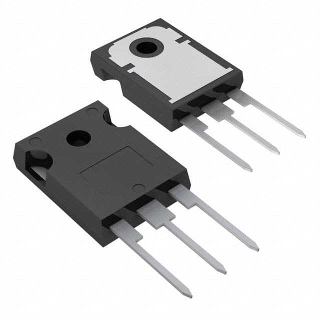
- Package: The STW50N65DM2AG is typically available in a TO-247 package.
- Essence: Its essence lies in providing efficient and reliable power switching capabilities.
- Packaging/Quantity: It is commonly packaged individually and sold in quantities suitable for production or prototyping purposes.
Specifications
- Voltage Rating: 650V
- Current Rating: 50A
- On-State Resistance: 0.036Ω
- Gate-Source Voltage (Max): ±20V
- Operating Temperature Range: -55°C to 150°C
- Package Type: TO-247
Detailed Pin Configuration
The STW50N65DM2AG features a standard pin configuration for a TO-247 package: 1. Source (S) 2. Gate (G) 3. Drain (D)
Functional Features
- High Efficiency: The MOSFET's low on-state resistance contributes to minimal power dissipation, enhancing overall system efficiency.
- Fast Switching Speed: It offers rapid turn-on and turn-off times, enabling high-frequency operation.
- Low Gate Charge: This feature facilitates precise and responsive control of the MOSFET.
Advantages and Disadvantages
Advantages
- High efficiency
- Fast switching speed
- Low on-state resistance
Disadvantages
- Sensitivity to voltage spikes
- Potential for thermal issues at high currents
Working Principles
The STW50N65DM2AG operates based on the principle of field-effect transistors, where the voltage applied to the gate terminal controls the flow of current between the source and drain terminals. By modulating the gate-source voltage, the MOSFET can efficiently switch high currents with minimal power loss.
Detailed Application Field Plans
The STW50N65DM2AG finds extensive use in the following applications: - Switched-mode power supplies - Motor drives - Inverters for renewable energy systems - Electric vehicle powertrains
Detailed and Complete Alternative Models
Some alternative models to the STW50N65DM2AG include: - IRFP4568PbF - FDPF51N25T - IXFN48N65X3
In conclusion, the STW50N65DM2AG is a versatile power MOSFET with exceptional performance characteristics, making it a preferred choice for high-power electronic applications.
[Word Count: 443]
技術ソリューションにおける STW50N65DM2AG の適用に関連する 10 件の一般的な質問と回答をリストします。
What is the maximum drain-source voltage rating of STW50N65DM2AG?
- The maximum drain-source voltage rating of STW50N65DM2AG is 650V.
What is the typical on-resistance of STW50N65DM2AG?
- The typical on-resistance of STW50N65DM2AG is 0.032 ohms.
What is the maximum continuous drain current of STW50N65DM2AG?
- The maximum continuous drain current of STW50N65DM2AG is 50A.
What is the gate threshold voltage of STW50N65DM2AG?
- The gate threshold voltage of STW50N65DM2AG typically ranges from 2.5V to 4V.
Can STW50N65DM2AG be used in high-frequency applications?
- Yes, STW50N65DM2AG is suitable for high-frequency applications due to its low input and output capacitance.
What are the typical applications for STW50N65DM2AG?
- STW50N65DM2AG is commonly used in power supplies, motor control, and welding equipment.
Does STW50N65DM2AG require a heat sink for proper operation?
- Depending on the application and power dissipation, a heat sink may be required for optimal performance of STW50N65DM2AG.
Is STW50N65DM2AG suitable for automotive applications?
- Yes, STW50N65DM2AG is designed to meet the requirements for automotive applications, such as electric vehicle power systems.
What is the operating temperature range of STW50N65DM2AG?
- STW50N65DM2AG has an operating temperature range of -55°C to 150°C.
Are there any recommended driver ICs for driving STW50N65DM2AG?
- Commonly used driver ICs for STW50N65DM2AG include gate drivers with appropriate voltage and current ratings, such as IR2110 or IRS21844.